• Ever wanted an RSS feed of all your favorite gaming news sites? Go check out our new Gaming Headlines feed! Read more about it here.
  • We have made minor adjustments to how the search bar works on ResetEra. You can read about the changes here.
Status
Not open for further replies.

z0m3le

Member
Oct 25, 2017
5,418
I doubt that Nvidia is planning to use the full Orin SOC at the 249$ price point unless it is a <200mm2 chip with a nintendo switch implementation in mind.
Should actually be somewhere around 120-140mm^2 on 5nm+, but I agree, cutting the CPU cores to 8, and dropping the cuda core count from ~1920 to 1280 or 1408 would be fine for a Switch successor, one benefit of using the full chip though is that they can actually come out with a cheaper part, and does sort of lean into what that road map is actually telling us, it seems like Nvidia wants to bin the parts, using the Switch successor to drive production of the SoC, and give higher performing parts to the high end automotive industry and defective parts to the low end AI industry. It could go either way, and the SoC could easily end up the same size as Tegra X1 (121mm^2).
 

Lelouch0612

Member
Oct 25, 2017
21,200
I don't believe a Pro is coming, a small budget tv box though sure.
Assuming it did happen though, i'm thinking just an upclocked TX1+.


Where did that pic come from?
So you find it more likely that the next revision will target budget consummers when the Lite is already doing that work ?

The Switch ASP is already down from 2017 and will go down even more in the future. A higher end model makes the most sense by far imo.
 

Onix555

Member
Apr 23, 2019
3,381
UK
So you find it more likely that the next revision will target budget consummers when the Lite is already doing that work ?

The Switch ASP is already down from 2017 and will go down even more in the future. A higher end model makes the most sense by far imo.
Lite is cheaper, but I feel there is a market for a $99-149 super budget sku with no portability. In addition we already have the Calcio firmware entry which sounds very similar.
 

Lelouch0612

Member
Oct 25, 2017
21,200
Lite is cheaper, but I feel there is a market for a $99-149 super budget sku with no portability. In addition we already have the Calcio firmware entry which sounds very similar.
I am not saying it is useless, it definitely has some purpose but it would be a niche revision.

The Pro would be the one to help "prolonge the life cycle of the Switch like no hardware before"
 

UltraMagnus

Banned
Oct 27, 2017
15,670
What would the performance on Tegra X1 die shrunk to 8nm possibly be?

Could it hit double the OG Switch docked (788 GFLOPS)?

If so maybe it's just that and Nano Next developer board would just be unused or faulty versions of that chip with 1/2 or 2/3 the CUDA cores. Current Nano board is 1/2 the Tegra X1.
 

z0m3le

Member
Oct 25, 2017
5,418
What would the performance on Tegra X1 die shrunk to 8nm possibly be?

Could it hit double the OG Switch docked (788 GFLOPS)?

If so maybe it's just that and Nano Next developer board would just be unused or faulty versions of that chip with 1/2 or 2/3 the CUDA cores. Current Nano board is 1/2 the Tegra X1.
So, just speculation on my part, but insiders seem to be relying on Tegra X1 profiles to match the Tegra X1 with the new model, however this doesn't rule out modifications to the Tegra X1 chip beyond a die shrink, it means it's still Maxwell/Pascal with A57 cores, but it could double the cuda core count for instance, and it is possibly built on 8nm as there is that Tegra 8nm rumor from earlier in the year. I think if this is the case, we should look at 800 to 900GFLOPs with 256 cuda cores or 1.3-1.6TFLOPs with 512 cuda cores. The reason I think they might have increased the cuda core count is simply because Nano hits that $129 price point by using chips that have disabled parts, such as Tegra X1 using 128 cuda cores instead of 256, or Xavier NX (a nano like design) using 384 cuda cores instead of 512.

It's not drastically changing the expectations of what this product would be, infact, 800 to 900 gflops puts it in low range XB1 parity, and 1.3-1.6tflops puts it in high range PS4 parity, in other words, it is still matching up with current generation base consoles, and we will have to wait 3 years from now to really see the successor.
 
Apr 11, 2020
1,235
Should actually be somewhere around 120-140mm^2 on 5nm+, but I agree, cutting the CPU cores to 8, and dropping the cuda core count from ~1920 to 1280 or 1408 would be fine for a Switch successor, one benefit of using the full chip though is that they can actually come out with a cheaper part, and does sort of lean into what that road map is actually telling us, it seems like Nvidia wants to bin the parts, using the Switch successor to drive production of the SoC, and give higher performing parts to the high end automotive industry and defective parts to the low end AI industry. It could go either way, and the SoC could easily end up the same size as Tegra X1 (121mm^2).
I'm asking my self if there is a chance of a $400 premium SKU in 2021 (running the 8 or 7 nm version of the 5 nm chip planned for 2023 lite and hybrid model) alongside two die shrunk TX1 SKUs (lite at $130~150 and hybrid at $250).

I find it hard to see Nintendo using a cuted version of Orin or even the entire chip. Especially on 8 nm (it may be too big?). However I would understand the choice to use the chip planned for the 2023 model on an older node in 2021 (7 nm is compatible with 5 nm) before moving on 5 nm for lite and hybrid in 2023 as they had done for TX1 (20 nm to 12 nm).
 
Last edited:

z0m3le

Member
Oct 25, 2017
5,418
I'm asking my self if there is a chance of a $400 premium SKU in 2021 (running the 8 or 7 nm version of the 5 nm chip planned for 2023 lite and hybrid model) alongside two die shrunk TX1 SKU model (lite at $130~150 and hybrid at $250).

I find it hard to see Nintendo using a cuted version of Orin or even the entire chip. Especially on 8 nm (it may be too big?). However I would understand the choice to use the chip planned for the 2023 model on an older node in 2021 (7 nm is compatible with 5 nm) before moving on 5 nm for lite and hybrid in 2023 as they had done for TX1 (20 nm to 12 nm).
Nvidia has 2 commercial SoC on their roadmap, Nano Next for 2021 (almost certainly a cut down Switch Pro SoC) and Orin a 2022 SoC with a 5 watt to 45 watt profile, spanning Jetson price points of $249 (same as Tegra X1/X2 when launched) to $899 (Xavier AGP price point).

That leaves little room for other chips IMO, and both are likely to be used by Nintendo, as Orin could be cut down or just downclocked and fully featured in the Switch successor, it's probably cheaper for Nvidia to produce 30 Million full size Orin chips a year, than 5 to 10 Million automotive full size Orin chips + 20 to 25 Million cut down Orin chips for a Switch successor.

As for price, Nintendo Switch is due for a price cut, so $349 for the Pro, current red box model $249 and Lite at $149.
 
Apr 11, 2020
1,235
Nvidia has 2 commercial SoC on their roadmap, Nano Next for 2021 (almost certainly a cut down Switch Pro SoC) and Orin a 2022 SoC with a 5 watt to 45 watt profile, spanning Jetson price points of $249 (same as Tegra X1/X2 when launched) to $899 (Xavier AGP price point).

That leaves little room for other chips IMO, and both are likely to be used by Nintendo, as Orin could be cut down or just downclocked and fully featured in the Switch successor, it's probably cheaper for Nvidia to produce 30 Million full size Orin chips a year, than 5 to 10 Million automotive full size Orin chips + 20 to 25 Million cut down Orin chips for a Switch successor.

As for price, Nintendo Switch is due for a price cut, so $349 for the Pro, current red box model $249 and Lite at $149.
It would be really interesting especially if the full Orin chip is really able to scale down to 5W in a Nintendo switch scenario.
 
Last edited:
Jul 14, 2020
606
So, just speculation on my part, but insiders seem to be relying on Tegra X1 profiles to match the Tegra X1 with the new model, however this doesn't rule out modifications to the Tegra X1 chip beyond a die shrink, it means it's still Maxwell/Pascal with A57 cores, but it could double the cuda core count for instance, and it is possibly built on 8nm as there is that Tegra 8nm rumor from earlier in the year. I think if this is the case, we should look at 800 to 900GFLOPs with 256 cuda cores or 1.3-1.6TFLOPs with 512 cuda cores. The reason I think they might have increased the cuda core count is simply because Nano hits that $129 price point by using chips that have disabled parts, such as Tegra X1 using 128 cuda cores instead of 256, or Xavier NX (a nano like design) using 384 cuda cores instead of 512.

It's not drastically changing the expectations of what this product would be, infact, 800 to 900 gflops puts it in low range XB1 parity, and 1.3-1.6tflops puts it in high range PS4 parity, in other words, it is still matching up with current generation base consoles, and we will have to wait 3 years from now to really see the successor.

Do you think increasing the count of CPU core is just as likely as increasing CUDA core count?

A doubling of cores all around and something near 1.6 tflops (+mixed precision) would actually be massive upgrade in my eyes.

Also, going from 400gflops to 1.6tflops would actually allow games that run at 900p-1080p to get close to 4K. Such a device would be about 2x as powerful as I currently expect.
 

Eslayer

Chicken Chaser
Member
Oct 27, 2017
330
if so maybe it's just that and Nano Next developer board would just be unused or faulty versions of that chip with 1/2 or 2/3 the CUDA cores. Current Nano board is 1/2 the Tegra X1.
I like the idea of Nano Next being a cut down version of whatever Nintendo would get, Originally I thought that if Nano Next was marginally better than Mariko that's what they would settle on
 

T002 Tyrant

Member
Nov 8, 2018
8,978
Nvidia has 2 commercial SoC on their roadmap, Nano Next for 2021 (almost certainly a cut down Switch Pro SoC) and Orin a 2022 SoC with a 5 watt to 45 watt profile, spanning Jetson price points of $249 (same as Tegra X1/X2 when launched) to $899 (Xavier AGP price point).

That leaves little room for other chips IMO, and both are likely to be used by Nintendo, as Orin could be cut down or just downclocked and fully featured in the Switch successor, it's probably cheaper for Nvidia to produce 30 Million full size Orin chips a year, than 5 to 10 Million automotive full size Orin chips + 20 to 25 Million cut down Orin chips for a Switch successor.

As for price, Nintendo Switch is due for a price cut, so $349 for the Pro, current red box model $249 and Lite at $149.

I hope that's certainly possible, especially if they use new materials to provide better thermal distribution too.

I am interested in Nate's theory on wireless docking too. I'm wondering if A VR solution could work where you had a wireless VR headset made from two 540p screens and used that additional power you're talking about to produce relatively decent VR experiences such as Pokémon Snap (imagine a March launch with a VR mode exclusive to the New Switch), RE7 and Thumper? The clocks could provide 1.6TFLOPS for a VR mode and say 1 - 1.3 for a "docked" mode (or the same as a VR mode depending on thermals). You could use the same wireless docking technology.

The only thing I can't put my finger on is the 4k, unless the 4k is being confused for the early specs of a Switch 2 dev kit?
 

z0m3le

Member
Oct 25, 2017
5,418
Do you think increasing the count of CPU core is just as likely as increasing CUDA core count?

A doubling of cores all around and something near 1.6 tflops (+mixed precision) would actually be massive upgrade in my eyes.

Also, going from 400gflops to 1.6tflops would actually allow games that run at 900p-1080p to get close to 4K. Such a device would be about 2x as powerful as I currently expect.
I am just trying to imagine what the Nvidia Nano Next is. I think the extra cuda cores makes sense for a Tegra device, while extra CPU clock speed should be enough to handle regular computations, Tegra Nano series is an entry level AI chip afterall.
I hope that's certainly possible, especially if they use new materials to provide better thermal distribution too.

I am interested in Nate's theory on wireless docking too. I'm wondering if A VR solution could work where you had a wireless VR headset made from two 540p screens and used that additional power you're talking about to produce relatively decent VR experiences such as Pokémon Snap (imagine a March launch with a VR mode exclusive to the New Switch), RE7 and Thumper? The clocks could provide 1.6TFLOPS for a VR mode and say 1 - 1.3 for a "docked" mode (or the same as a VR mode depending on thermals). You could use the same wireless docking technology.

The only thing I can't put my finger on is the 4k, unless the 4k is being confused for the early specs of a Switch 2 dev kit?
The PS3 is capable of 4K. Tegra X1 is also capable of 4K, I think just internal upscaling, and while I think it is possible something like doubling cuda cores could happen, I wouldn't expect it, I'm digging for more information and I'll try to come up with more credible stuff, but in the meantime, it's just about what Nano Next could be, I think we could see it at GTC this October 5th, Nvidia has a keynote and they could talk more about nano next there.

I still mostly believe the Switch 'Pro' is 800 to 900 gflops, I'm just bringing up whatever I can think of to address this new SoC, which I believe ultimately is a cut down Switch Pro SoC.
 
Last edited:

z0m3le

Member
Oct 25, 2017
5,418
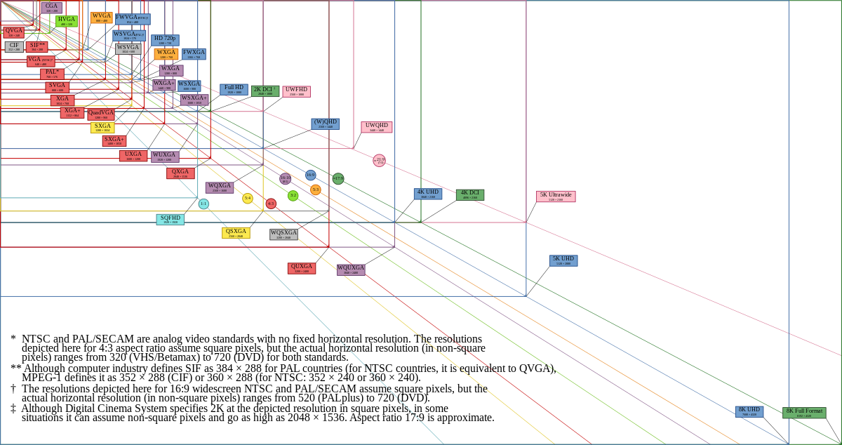
These are all marketing terms that mean nothing. 2K meaning 2000+x1440p is closer to a usable resolution than the ones in that wiki because the ratios are 3:2 not 1:2, or with the case of 2560x1440p, it is 16:9, the standard ratio of a TV.

4k is specifically talking about it's horizontal resolution, which is why 1440p being considered 2K isn't wrong, if we ask Google:
Is 1440p 2k or 4k?
Yes, 2560x1440 monitors (1440p) are commonly referred to as 2k monitors. They have nearly twice the pixels as 1920x1080 (1080p or full HD) monitors do.
 
Dec 23, 2017
8,802
Been thinking about this. I mean we know Nintendo are big on NDA's but if this is realeasing really Q1 or Q2 of next year shouldn't developers already have this in hand working on making games and ports? Unless they are using switch dev kits up locked to somewhat off set what this upgrade will provide? That is curious to me.
 

z0m3le

Member
Oct 25, 2017
5,418
Been thinking about this. I mean we know Nintendo are big on NDA's but if this is realeasing really Q1 or Q2 of next year shouldn't developers already have this in hand working on making games and ports? Unless they are using switch dev kits up locked to somewhat off set what this upgrade will provide? That is curious to me.
There is a rumor that some developers have at least seen it, but honestly external developers don't really need to see something like this until 5 or 6 months out. Even then, it's not mandatory for 3rd party games to utilize this new hardware, dynamic resolution would still be effected, so many games would still see a huge benefit.
 

ShadowFox08

Banned
Nov 25, 2017
3,524
I commented on the Bloomberg thread before about that Jetson roadmap, and I'll say it again here:

The TX2 8GB Jetson module has me intrigued. It has 59.7GB/s Ram and shares the same 4 CPU A57 cores as TX1, as well as the 7-15 watt profile and similar die size. I don't see why Nintendo can't just use a 7-8nm die shrink of the TX2 and disable the Denver cores. They could go further replace the LPDDR4 ram with LPDDR4x and use 128 bit buswidth or LPDDR5 with 64 bit bus width to save more energy. Then they boost CPU and GPU clock by 2x.

By making a die shrink of TX2 instead of TX1, you get more cache, already 8GB as the default, at least 59.7 GB/s speed (dunno how they achieve it) from, and you already have A57 cores. Like the A53s, the Denver's will be disabled. Of course, I would wish they go further and just replace the Denver (or A53s for TX1) and have more A57 cores. Anyway, using a die shrink of TX2 is more feasible than Xavier NX. Less customization required.
 
Apr 11, 2020
1,235
Been thinking about this. I mean we know Nintendo are big on NDA's but if this is realeasing really Q1 or Q2 of next year shouldn't developers already have this in hand working on making games and ports? Unless they are using switch dev kits up locked to somewhat off set what this upgrade will provide? That is curious to me.
You don't need to deliver a new devkit if your handheld mode is just the OG model max clocks.
 
Apr 11, 2020
1,235
I commented on the Bloomberg thread before about that Jetson roadmap, and I'll say it again here:

The TX2 8GB Jetson module has me intrigued. It has 59.7GB/s Ram and shares the same 4 CPU A57 cores as TX1, as well as the 7-15 watt profile and similar die size. I don't see why Nintendo can't just use a 7-8nm die shrink of the TX2 and disable the Denver cores. They could go further replace the LPDDR4 ram with LPDDR4x and use 128 bit buswidth or LPDDR5 with 64 bit bus width to save more energy. Then they boost CPU and GPU clock by 2x.
Isn't Mariko already using LPDDR4X?
 

Mr.Gamerson

Member
Oct 27, 2017
906
1080p locked 30fps BOTW 2 with maybe HDR added is a big enough upgrade for Zelda but if Nintendo was able to make the Pro strong enough to get BOTW 2 running at 900p/1080p dynamic at 60fps, it would help a lot to market the visual improvements of the game when compared to base switch. I think the difference between 900p vs 1080p is much smaller when compared to 30fps vs 60fps side by side.
 

Pokemaniac

Member
Oct 25, 2017
4,944
Been thinking about this. I mean we know Nintendo are big on NDA's but if this is realeasing really Q1 or Q2 of next year shouldn't developers already have this in hand working on making games and ports? Unless they are using switch dev kits up locked to somewhat off set what this upgrade will provide? That is curious to me.
Possibly a handful of key 3rd parties have dev kits by now, but there's much less of a need for early dev kits for a revision like this, since it isn't a full new platform. Unless the dev is working on an exclusive title, they can just continue to target the current Switch for now (since they'll have to do that anyway), then adjust things for Switch Pro once kits become available.
 

Whatnoww

Member
Jun 26, 2019
133
I have a thought. And this has to do with that recent release from the FCC in which Nintendo filed to change the SOC and RAM this year.

IF Nintendo uses a die shrunk 7nm Tegra X1, and doubles the bandwidth either by offering 128 bus width RAM of lddr4x, or going straight to 64 bit LPDDR5... It's already being customized enough, so what's stopping Nintendo and Nvidia from replacing the A53s with more A57s and upclocking them? Perhaps have 6 cores at say 1.5 GHz, with one reserved for OS? That's already happens to r 2.5x performance of current switch CPU, and right in the ballpark of xbone and ps4 base models. If Nintendo could do it with new 3ds, they could do it with the switch 2021?

I say A57 due to easy compatibility, despite newer models existing, at least the former doesn't need to be set to different clockspeeds, which requires even more work and additional profiles for devs.

That's if Nintendo decides on a 7nm TX1 and goes the new 3DS route with the RAM and CPU. upgrade. They could also do 1.5 to 2Ghz CPUs and still have useless A53 space for nothing, and have 1.5 to 2x the performance for the A57s too, but the CPU would still be a bit of a bottleneck then on the he lower end.

This could probably be possible, especially considering it would make all of the 8 cores available, maybe deserving a newer Tegra X1++ renaming. If they go all the way and replace the CPU portion of the SoC, chances are they'll go with the typical 4xA78 with backwards compatibility being taken care of higher clocked 4xA57s. It really goes to show how backwards compatibility is insanely easy considering newer SoC's are still using A57's as efficiency cores.
 

Dakhil

Member
Mar 26, 2019
4,459
Orange County, CA
This could probably be possible, especially considering it would make all of the 8 cores available, maybe deserving a newer Tegra X1++ renaming. If they go all the way and replace the CPU portion of the SoC, chances are they'll go with the typical 4xA78 with backwards compatibility being taken care of higher clocked 4xA57s. It really goes to show how backwards compatibility is insanely easy considering newer SoC's are still using A57's as efficiency cores.
The problem is that the Cortex-A57, unlike the Cortex-A78, doesn't support DynamIQ. The Cortex-A57 supports Arm big.LITTLE, which doesn't allow heterogeneous CPU cores to be used simultaneously, which is the reason why the Cortex-A53 is disabled in the Tegra X1+.
 

Whatnoww

Member
Jun 26, 2019
133
These are all marketing terms that mean nothing. 2K meaning 2000+x1440p is closer to a usable resolution than the ones in that wiki because the ratios are 3:2 not 1:2, or with the case of 2560x1440p, it is 16:9, the standard ratio of a TV.

4k is specifically talking about it's horizontal resolution, which is why 1440p being considered 2K isn't wrong, if we ask Google:
Is 1440p 2k or 4k?
Yes, 2560x1440 monitors (1440p) are commonly referred to as 2k monitors. They have nearly twice the pixels as 1920x1080 (1080p or full HD) monitors do.

Google pulls sources from any random website, and most of them are wrong. A reasonable explanation is this one. https://linustechtips.com/main/topic/691408-2k-does-not-mean-2560×1440/

Issue is that if you use 2K in that sense, you would be both referring to a 1080p monitor and a 1440p monitor if you were to use them interchangebly. 2K doesn't mean double 1080p. In cinema, 1440p is usually 2.5K.
 

Whatnoww

Member
Jun 26, 2019
133
The problem is that the Cortex-A57, unlike the Cortex-A78, doesn't support DynamIQ. The Cortex-A57 supports Arm big.LITTLE, which doesn't allow heterogeneous CPU cores to be used simultaneously, which is the reason why the Cortex-A53 is disabled in the Tegra X1+.

Interesting. I was confusing them with the other low power cores. It would probably make more sense to go with the entire 8xA57 cluster, though that feels dubious. If they're changing it, why not go for a higher performance upgrade, which won't cost much more but would give huge benefits?
 

MP!

Member
Oct 30, 2017
5,198
Las Vegas
These are all marketing terms that mean nothing. 2K meaning 2000+x1440p is closer to a usable resolution than the ones in that wiki because the ratios are 3:2 not 1:2, or with the case of 2560x1440p, it is 16:9, the standard ratio of a TV.

4k is specifically talking about it's horizontal resolution, which is why 1440p being considered 2K isn't wrong, if we ask Google:
Is 1440p 2k or 4k?
Yes, 2560x1440 monitors (1440p) are commonly referred to as 2k monitors. They have nearly twice the pixels as 1920x1080 (1080p or full HD) monitors do.
lets not forget as well that those terms in the development world for textures is different as well ...
1k 1024x1024
2k 2048x2048
4k 4096x4096
and so on...
I kind of find it funny that we still don't have a consistent naming convention for this stuff...
lets not even get into measuring stuff in Megapixels lol
 

bmfrosty

Member
Oct 27, 2017
1,894
SF Bay Area
Jul 14, 2020
606
There is. (Scroll all the way down until you see 2019-07-09.)
Yes, I believe there was one a year ago with changes to the SOC and RAM. Besides the 12/16nm die shrink from 20nm, the only thing I saw changed besides smaller CPU cores were the LPDDR4x RAM.

Thanks. Do we know much smaller the Mariko die is? I can easily find that the t210 was 118mm^2 but google isn't feeding me any helpful results for Mariko.
 

Onix555

Member
Apr 23, 2019
3,381
UK
After comparing the two I believe it's just a TX1+
5yMqol0.jpg


Same amount and positions of capacitors.

EDIT:
In addition heres a TX1vs+ comparison I made for no real reason.
NsPpsLb.jpg
 
Last edited:

Dakhil

Member
Mar 26, 2019
4,459
Orange County, CA
so would it be safe to assume that our baseline is another die shrink? (and maybe more ram?)
I think a die shrunk Tegra X1+ is a reasonable assumption. And I guess the new Nintendo Switch model might go for faster RAM (either by using LPDDR5 on a 64-bit memory bus width, or by using LPDDR4X, but with a 128-bit memory bus width, instead of the 64-bit memory bus width on the current Nintendo Switch model) over more RAM.
 

MP!

Member
Oct 30, 2017
5,198
Las Vegas
I think a die shrunk Tegra X1+ is a reasonable assumption. And I guess the new Nintendo Switch model might go for faster RAM (either by using LPDDR5 on a 64-bit memory bus width, or by using LPDDR4X, but with a 128-bit memory bus width, instead of the 64-bit memory bus width on the current Nintendo Switch model) over more RAM.
that would really help the two biggest bottlenecks with switch.
 

Kingpin722

Member
Oct 28, 2017
1,028
NVIDIA just updated their latest Shield TVs with better AI upscaling. Could possibly be more evidence of them working on Implementing it into Switch Pro. Hopefully.
 

Dakhil

Member
Mar 26, 2019
4,459
Orange County, CA
Could they issue a new dock or would that require a separate patent?
I'm guessing if the chips on the dock have changed, Nintendo would have to mention that to the FCC when making a FCC filing. And given the FCC filing that was made public on 23 August 2020 is very similar to the FCC filing that was made public on 9 July 2019, I think it's reasonable to assume the dock for the new Nintendo Switch model is the same as the dock for the current Nintendo Switch model (the revised model).

NVIDIA just updated their latest Shield TVs with better AI upscaling. Could possibly be more evidence of them working on Implementing it into Switch Pro. Hopefully.
If I recall correctly, the AI upscaling on the Nvidia Shield TV only applies to media. And despite the fact that the current Nintendo Switch model and the Nvidia Shield TV share the same SoC, I believe the current Nintendo Switch model doesn't take advantage of AI upscaling when watching media (like on YouTube). So I don't think the AI upscaling on the Nvidia Shield TV will be brought over to the new Nintendo Switch model.
 
Status
Not open for further replies.