• Ever wanted an RSS feed of all your favorite gaming news sites? Go check out our new Gaming Headlines feed! Read more about it here.

What do you think could be the memory setup of your preferred console, or one of the new consoles?

  • GDDR6

    Votes: 566 41.0%
  • GDDR6 + DDR4

    Votes: 540 39.2%
  • HBM2

    Votes: 53 3.8%
  • HBM2 + DDR4

    Votes: 220 16.0%

  • Total voters
    1,379
Status
Not open for further replies.

Pheonix

Banned
Dec 14, 2018
5,990
St Kitts
This is why insiders stop posting here ....people are way to over zealous and twist what people say over their fan war. It's ridiculous
Why are you quoting me?

Or me saying confirming something like BC for a PS5 isn't a big deal is beng over zealous?

I mean considering how big digital distribution has become this gen, not having BC would be a catastrophic mistake. You don't need insider knowledge to know that. I know I have 'NEVER" said anything about Matt before. Or even mentioned him until that post. And that was for the reasons stated in the post. BC is a no brainer. That's like saying there will be a disc drive in the next-gen consoles.
 

TheRealTalker

Member
Oct 25, 2017
21,450
The PS5 is Gogeta Blue and the X2 is Broly fully powered
EkNucew.gif
 

gundamkyoukai

Member
Oct 25, 2017
21,087
Why are you quoting me?

Or me saying confirming something like BC for a PS5 isn't a big deal is beng over zealous?

I mean considering how big digital distribution has become this gen, not having BC would be a catastrophic mistake. You don't need insider knowledge to know that. I know I have 'NEVER" said anything about Matt before. Or even mentioned him until that post. And that was for the reasons stated in the post. BC is a no brainer. That's like saying there will be a disc drive in the next-gen consoles.

It was expected for me also but a lot of people did not think it was going to happen.
Reasons being no BC for PS4 or there were not certain because Sony has not really care about BC much this gen .
So matt post for them was more insight , just like how he said X would not have zen and some people went crazy lol.
 
Oct 25, 2017
1,844
honestly? I think right now they want to talk about power, and xCloud. so they're likely simply ignoring or choosing not to mention a potential lower powered sku. They've only shown beauty shots of a CG motherboard and no name/box/controller has been shown so its still very early.

Doesn't mean anything at this point IMO
They also haven't shown any Next Gen exclusive games.

Given BC support/Cross-gen titles, without a Next Gen exclusive that would require either the Anaconda or Lockhart, there's no way to sell/differentiate Lockhart from the already available X. So it makes sense not to talk about it.
 

Deleted member 17092

User requested account closure
Banned
Oct 27, 2017
20,360
I think we will see RT reflections and 4k checker boarding. GI is just way too taxing. A heavily ocd 2070 does metro at like a .6 4k resolution scale and high settings at like 40-60fps with heavy drops in more intense areas.

I can't see a ton of console games going the GI route unless they go with 1080p, which honestly probably makes the most sense as TVs have very good scalers vs monitors.

And GI is actually worth the res and fps drop, where reflections are kinda meh. Devs have gotten very good at prebaked lighting so honestly I don't care all that much about RT unless it's GI. And we're basically 1-2 gpu gens away still from having an affordable (sub $500) discrete you that can pull off GI at 4k60.

Y'all are kind of expecting too much from RT imo unless we do see some pretty custom shit that even NV has yet to figure out.
 

DukeBlueBall

Banned
Oct 27, 2017
9,059
Seattle, WA
I think we will see RT reflections and 4k checker boarding. GI is just way too taxing. A heavily ocd 2070 does metro at like a .6 4k resolution scale and high settings at like 40-60fps with heavy drops in more intense areas.

I can't see a ton of console games going the GI route unless they go with 1080p, which honestly probably makes the most sense as TVs have very good scalers vs monitors.

And GI is actually worth the res and fps drop, where reflections are kinda meh.

It's possible that AMD RT scales with scene complexity instead of resolution.
 

Deleted member 17092

User requested account closure
Banned
Oct 27, 2017
20,360
A year and half is a long time. NV's solution would be improved before a year and half pass.

Well yeah, I have faith NV will make dramatic improvements to their RT tech in a year and a half. Amd sure but that's only because they have literally nothing for RT and they still can't make a gpu that's any better than a 1080 ti, a now 2+ year old gpu.
 

Liabe Brave

Professionally Enhanced
Member
Oct 27, 2017
1,672
1) Am I correct in assuming that the word, "Binning" and "down-grading" are interchangeable insofar as disabling parts of the product because 100% of its constituent core components are not fully functional? And so presumably, every semi-custom APU powering the X, is binned given 4CUs are disabled within the GPU.
I'll try to answer as I can, though I have only a layman's knowledge of silicon production.

I don't know the true etymology of "binning", but I've always assumed it was an analogy (or maybe an actual physical activity!) of separating dice into bins. It's driven by faults in the physical structure of supposedly identical chips, presumably caused by crystal defects, vapor deposition variability, etc. Some faults are so bad that they make functional blocks unusable. Some are less serious and can be made to work by adjusting the voltage of the current running through them. But overvolting or undervolting to accommodate the flaw may cause the rest of the chip to stop working, so there's a limit.

Silicon is expensive (I think I've heard estimates like $15k for a single 300mm wafer?). So you don't want to just throw away the chips with parts which don't work, or chips that need altered voltage. By designing an end product which uses the perfect chips, and another which uses partially disabled chips, you can still sell the defective parts. As long as the number of faulty CUs doesn't exceed the number you ignore anyway, you can use the chip. For example, Navi 5700XT uses all 20 WGPs/40 CUs, whereas Navi 5700 is the exact same chips but with 2 WGPs/4 CUs disabled.

As for power variability, a certain amount can be tolerated by normal power supplies, and fans can be driven at different speeds by software. The range covered is relatively small, but you don't have to customize each console's hardware for this. That's why different users' consoles can reach different temperatures or noise levels (due to cooling needs): they're drawing and dissipating different amounts of power. The Hovis Method widens the acceptable range, presumably by a significant amount.

2) Does Hovis method means that each X mobo is individually tested at specific nodes to check for voltage (or amperage) against a reference and when variability is found for a specific junction/junctions, the power profile is customized to ensure extra power is delivered to those specific areas to compensate for shortfall, ensuring exact performance across all finished products?
I don't think specifics are known, or at least I haven't heard any. From what I do understand, One X has a bank of extra capacitors in the traces leading to the APU, so presumably turning these off or on for specific machines does basically what you say, "fingerprinting" the power to particular die needs. I'd wager the Hovis hardware itself is identical across all motherboards, with the profile of which caps to use stored in a profile.

If so, would this not mean that that yields for regular One, PS4 Slim and Pro would be worse if variance in voltage at certain nodes is discovered at testing phase (i.e. mobo with all the integral parts soldered on) and that entire assembled product would have been abandoned? Because if not, does it not inherently mean that not all the aforementioned models perform equally?
Even if the testing is done with final boards rather than a rig (which I'm not sure about), I imagine they'd just demount the chip rather than discard the entire assembly. And consoles don't perform equally--for some definitions of "perform". During testing, the constant standard that's being checked against is "Can this chip operate at a specific clock with [x] amount of silicon active?" The amount of power necessary to make it operate is what's adjusted. So a specific PS4 may get less TF per watt, and by that sense perform worse...but it still hits the exact same TF number as its brethren.

A pleasure to see you here. Is there anything you can share about hopes or needs for raytracing or other new techniques on the coming machines? What parts of the job would benefit most, and how likely is it the necessary support will materialize? Will the extra capacity increase or reduce the time necessary to create? Understood that anything you say is only your own thoughts, not an official stance.
 
Oct 27, 2017
7,135
Somewhere South
I just hope that whatever RT solution both consoles have implemented is flexible, that it isn't constrained to traversing specific data structures like BVHs, for instance. There's an universe of dynamic GI solutions out there that can get you pretty good results at a fraction of the computational cost of traditional path tracing.
 

Deleted member 17092

User requested account closure
Banned
Oct 27, 2017
20,360
I'll try to answer as I can, though I have only a layman's knowledge of silicon production.

I don't know the true etymology of "binning", but I've always assumed it was an analogy (or maybe an actual physical activity!) of separating dice into bins. It's driven by faults in the physical structure of supposedly identical chips, presumably caused by crystal defects, vapor deposition variability, etc. Some faults are so bad that they make functional blocks unusable. Some are less serious and can be made to work by adjusting the voltage of the current running through them. But overvolting or undervolting to accommodate the flaw may cause the rest of the chip to stop working, so there's a limit.

Silicon is expensive (I think I've heard estimates like $15k for a single 300mm wafer?). So you don't want to just throw away the chips with parts which don't work, or chips that need altered voltage. By designing an end product which uses the perfect chips, and another which uses partially disabled chips, you can still sell the defective parts. As long as the number of faulty CUs doesn't exceed the number you ignore anyway, you can use the chip. For example, Navi 5700XT uses all 20 WGPs/40 CUs, whereas Navi 5700 is the exact same chips but with 2 WGPs/4 CUs disabled.

As for power variability, a certain amount can be tolerated by normal power supplies, and fans can be driven at different speeds by software. The range covered is relatively small, but you don't have to customize each console's hardware for this. That's why different users' consoles can reach different temperatures or noise levels (due to cooling needs): they're drawing and dissipating different amounts of power. The Hovis Method widens the acceptable range, presumably by a significant amount.


I don't think specifics are known, or at least I haven't heard any. From what I do understand, One X has a bank of extra capacitors in the traces leading to the APU, so presumably turning these off or on for specific machines does basically what you say, "fingerprinting" the power to particular die needs. I'd wager the Hovis hardware itself is identical across all motherboards, with the profile of which caps to use stored in a profile.


Even if the testing is done with final boards rather than a rig (which I'm not sure about), I imagine they'd just demount the chip rather than discard the entire assembly. And consoles don't perform equally--for some definitions of "perform". During testing, the constant standard that's being checked against is "Can this chip operate at a specific clock with [x] amount of silicon active?" The amount of power necessary to make it operate is what's adjusted. So a specific PS4 may get less TF per watt, and by that sense perform worse...but it still hits the exact same TF number as its brethren.


A pleasure to see you here. Is there anything you can share about hopes or needs for raytracing or other new techniques on the coming machines? What parts of the job would benefit most, and how likely is it the necessary support will materialize? Will the extra capacity increase or reduce the time necessary to create? Understood that anything you say is only your own thoughts, not an official stance.

I've actually often wondered about this with consoles. Like I assume thermal throttling does actually happen on some consoles more than others given the silicon lottery. You're saying that isn't the case?

Like if a chip is hardwired to throttle at 85 C, and say one Xbox one x hits that and throttles, but another Xbox one x does not hit that so it doesn't throttle. So theoretically a given Xbox one x may see more fps dips than another? Or no?
 
Oct 27, 2017
7,135
Somewhere South
I've actually often wondered about this with consoles. Like I assume thermal throttling does actually happen on some consoles more than others given the silicon lottery. You're saying that isn't the case?

Like if a chip is hardwired to throttle at 85 C, and say one Xbox one x hits that and throttles, but another Xbox one x does not hit that so it doesn't throttle. So theoretically a given Xbox one x may see more fps dips than another? Or no?

Consoles don't throttle. They have their cooling designed to deal with sustained loads at their designated max frequency. If they detect they're overheating for some reason (say, ambient temperatures that are way too high, hampered air flow, etc), they generally just shut down.
 

Deleted member 1589

User requested account closure
Banned
Oct 25, 2017
8,576
Anthony Hopkins spinning Matt's quote that PS5 has RT hardware to it probably being Sony bending the truth was a sight.

I'm glad some of the discussions went on while I was sleeping though. I can't believe how badly some took Reiner's tweet.
 

Deleted member 17092

User requested account closure
Banned
Oct 27, 2017
20,360
Consoles don't throttle. They have their cooling designed to deal with sustained loads at their designated max frequency. If they detect they're overheating for some reason (say, ambient temperatures that are way too high, hampered air flow, etc), they generally just shut down.

Hmm interesting. Thanks!

Curious though, has there been any documented substantial independent testing on this subject?

Like has anyone grabbed like 100+ random Xbox one xs or ps4 pros and tested them?

Like I kind of have a feeling there would be a significant amount of variance in fps on the most taxing titles.
 

Pheonix

Banned
Dec 14, 2018
5,990
St Kitts
It was expected for me also but a lot of people did not think it was going to happen.
Reasons being no BC for PS4 or there were not certain because Sony has not really care about BC much this gen .
So matt post for them was more insight , just like how he said X would not have zen and some people went crazy lol.
Idk.... but the PS4 not having PS3 BC was no surprise to me. Considering the cell. But for the PS5 having BC was pretty much a no brainer especially when you consider its also based on an x86 architecture.

Look, I 'm not knocking the guy so I don't know why you are taking issue with me. All I am saying is that "leaking" BC isn't something that impresses me. (and that's if all the patents that were making the rounds for years didn't tell you that already.)

If it would make you feel better I don't believe nor dispute any leaks or rumor from anyone. Matt, Jason, Reiner, Brad... not a single one of them. I just won't either come out and cal any of them a liar too.
 
Oct 27, 2017
7,135
Somewhere South
Hmm interesting. Thanks!

Curious though, has there been any documented substantial independent testing on this subject?

Like has anyone grabbed like 100+ random Xbox one xs or ps4 pros and tested them?

I don't think I've ever seen anything like that, but I remember that back in the day - 2007 or 2008, I think - I've read some testing with both the PS3 and X360 to see how much heating it would take for them to shut down (combo of sustained loads + ambient heat). Can't remember the exact numbers, but it was way north of 40°C ambient for both.

Like I kind of have a feeling there would be a significant amount of variance in fps on the most taxing titles.

There won't be any significant difference in FPS, actually, because consoles don't throttle. What will happen is that some consoles that sit at the extremes of what's acceptable silicon will have their fans spinning at full tilt sooner and more often.
 
Last edited:

gundamkyoukai

Member
Oct 25, 2017
21,087
Idk.... but the PS4 not having PS3 BC was no surprise to me. Considering the cell. But for the PS5 having BC was pretty much a no brainer especially when you consider its also based on an x86 architecture.

Look, I 'm not knocking the guy so I don't know why you are taking issue with me. All I am saying is that "leaking" BC isn't something that impresses me. (and that's if all the patents that were making the rounds for years didn't tell you that already.)

If it would make you feel better I don't believe nor dispute any leaks or rumor from anyone. Matt, Jason, Reiner, Brad... not a single one of them. I just won't either come out and cal any of them a liar too.

I am not taking issue with you .
Just saying that what you thought was not impressive other people thought other wise since he said that in the gaf days and some people trust in Sony having BC was low .
For me BC was going happen because the change to x86, DD , GaaS and Sony has history of BC that people ignore without looking at the context .
 

Deleted member 17092

User requested account closure
Banned
Oct 27, 2017
20,360
I don't think I've ever seen anything like that, but I remember that back in the day - 2007 or 2008, I think - I've read some testing with both the PS3 and X360 to see how much heating it would take for them to shut down (combo of sustained loads + ambient heat). Can't remember the exact numbers, but it was way north of 40°C ambient for both.

See then imo if there isn't any independent testing I actually think there's a pretty good chance that this is happening just based on how AMD and Nvidia chips work. They'll throttle if they need to.

If I had like $5k to blow I'd do it. Maybe DF could do it.
 

Deleted member 17092

User requested account closure
Banned
Oct 27, 2017
20,360
I don't think I've ever seen anything like that, but I remember that back in the day - 2007 or 2008, I think - I've read some testing with both the PS3 and X360 to see how much heating it would take for them to shut down (combo of sustained loads + ambient heat). Can't remember the exact numbers, but it was way north of 40°C ambient for both.


There won't be any significant difference in FPS, actually, because consoles don't throttle. What will happen is that some consoles that sit at the extremes of what's acceptable silicon will have their fans spinning at full tilt sooner and more often.

I mean sure but you're saying that without any testing.

Various gpus of the exact same model and board partner even with much beefier air cooling at 100% fans will perform differently. Unless Sony and Ms are binning their chips much more selectively than amd and Nvidia board partners (which I really doubt given the pure volume), I'd expect some variance.

Like basically you're saying they've binned the chips so we'll there is a Zero percent chance of thermal throttling. I don't really believe that especially without any 3rd party testing when the standard practice of AMD in the PC space is that their gpus don't even hit anywhere near advertised clocks without adjusting the fan curve and also undervolting. Like their chips do get hot and they do throttle, and it seems like that would be even more prevalent in a small console box.

Like if we're just relying on and/Sony/Ms word on this I don't really buy it without significant testing.

I mean serious question has anyone even tested the actual clock rates at load of a Sony or Ms console this gen on a level with a good sample size?
 
Last edited:

Dave.

Member
Oct 27, 2017
6,139
I mean sure but you're saying that without any testing.

Various gpus of the exact same model and board partner even with much beefier air cooling at 100% fans will perform differently. Unless Sony and Ms are binning their chips much more selectively than amd and Nvidia board partners (which I really doubt given the pure volume), I'd expect some variance.

Like basically you're saying they've binned the chips so we'll there is a Zero percent chance of thermal throttling. I don't really believe that especially without any 3rd party testing when the standard practice of AMD in the PC space is that their gpus don't even hit anywhere near advertised clocks without adjusting the fan curve and also undervolting. Like their chips do get hot and they do throttle, and it seems like that would be even more prevalent in a small console box.

Like if we're just relying on and/Sony/Ms word on this I don't really buy it without significant testing.

I mean serious question has anyone even tested the actual clock rates at load of a Sony or Ms console this gen on a level with a good sample size?

Consoles don't boost though. When you see an modern PC GPU "thermal throttle", what you actually see is it not boosting quite so high above base clock. They never throttle below base, you only ever get "a bit less extra". When you say "advertised clocks" you mean max boost clocks - no un-faulty GPU has trouble holding it's base clocks indefinitely ever.

Consoles would rather endure the heat and if it gets too much pop a warning on screen and shut down rather than give inconsistent performance.
 

Liabe Brave

Professionally Enhanced
Member
Oct 27, 2017
1,672
Like basically you're saying they've binned the chips so we'll there is a Zero percent chance of thermal throttling.
No he isn't. He's saying that instead of throttling, consoles just shut off when they get very hot. The manufacturers know exactly what dissipation to expect because there's no such thing as overclocking or fan curve adjustments by users.

Also, though it isn't a giant sample size, major console games sometimes do have their framerates analyzed by multiple outlets. I've never seen significant discrepancies between the results. In addition, playing backwards-compatible games on Xbox One S and One X often shows commensurate performance variability curves during identical loads like cutscenes. This would be a strange coincidence if both devices independently varied from their standard profile.
 

Dave.

Member
Oct 27, 2017
6,139
I don't think specifics are known, or at least I haven't heard any. From what I do understand, One X has a bank of extra capacitors in the traces leading to the APU, so presumably turning these off or on for specific machines does basically what you say, "fingerprinting" the power to particular die needs. I'd wager the Hovis hardware itself is identical across all motherboards, with the profile of which caps to use stored in a profile.

Anexanhume posted this not so long ago:


Detective

Member
Oct 27, 2017
3,852
This thread..WOW

Albert Penello thanks for being here sharing your knowledge and expertise, much appreciated!

For me, rumors are rumors no matter how good, bad, reliable there are. They are just rumors. I Don't believe in any of them.

I take everything as a rumor if it's not by the original official source and that is MS or Sony.
 

GhostTrick

Member
Oct 25, 2017
11,304
Not even close. I pointed out why they wont be going for a 350mm2 chip anymore. If they are going for a bigger chip, they are going for more CUs. If they are going for more CUs, they have already accounted for the tdp increases and added cooling solutions to account for it.

Previous facts are great, but if we go by previous facts then we have to assume that Sony would be going with a $399 350mm2 console. They are almost assuredly not.

If we go by previous facts, we would assume that MS would settle for a 350mm2 vapor cooled system. The estimates already prove that this is no longer the case and that MS was able to get an even bigger die for the same price.

If we go by pervious facts, Sony would settle for a 325mm2 APU like they did for the pro.

Another cool previous fact: the PS3 shipped with a 395w power supply and had games go over 200W during gameplay. PS4 topped out at 150w during gameplay. If Sony is going for $499, why cant they have another 200w console? The bluray drive wont be consuming any power because the games will all be installed on the SSD.

Things have changed. We have an SSD in next gen consoles. We are going to get hardware RT. two months ago, everyone thought this was crazy. two weeks ago, everyone though navi was GCN. lets not rely on previous facts too much. Lets wait and see what the next Navi GPUs can do because in all likelyhood next gen consoles are using those chips instead.


RX 5700 XT: 251mm2
HD7870: 212mm2
RX 580: 232mm2

Sorry, RX 5700 is bigger.
 

AegonSnake

Banned
Oct 25, 2017
9,566
And before you try to come up with reasons to say how this not economically feasible or that it's not possible because of heat or power consumption, consider this...
We've spent literally tens of thousands of posts being told pretty confidently the following:
- You will be lucky if you've got machines capable of 8 or 10 GCN TFLOPS
- SSDs are a pipe dream.
- There's zero chance consoles will have ray-tracing.
You've been wrong on all counts. Hell, I believed two of those three points. But we're wrong. So... Maybe it's about time we consider that these machines will not be designed in the same way the previous gen's consoles were made. Crazy idea, huh?
i wanted to piggyback on this for a second. it's been crazy how just a few months ago, we were split into two camps in regards to SSDs. RT was a pipe dream. And team 12 GCN tflops was mocked and a good chunk of this thread took the 8 tflops rumors seriously. this is back when the architectural improvements were supposed to be 10% at best. even then we had i'd say half of the thread convinced ps5 was going to be 8 GCN tflops. no we are up to 9-10 rdna tflops which are apparently better than 12.6 gcn tflops by 10%. so more like 14 tflops.

So SSD, hardware RT, brand new RDNA arch, and for the first time in the history of both consoles, a $499 price tag for a console dedicated for gaming and devoid of any kind of bullshit camera or bluray hardware. no offense to the x1x, but it was likely sold at a profit. these consoles will likely be sold at a loss so we are looking at a BOM of $500.

409628-ihs-xbox-one-teardown.jpg

what can MS do with the $75 they wasted on kinect last gen? sony has a full $100 to play with. vapor chamber shouldnt cost more than $10-20 extra on top of standard cooling. so they have $80-90 to spend on a bigger APU. i doubt SSDs are going to be as cheap as $37 so lets add $20, you still have $60-70 for the APU. a $170 APU can do amazing things.

Lastly, up until last week, we all assumed Anaconda was going to be more powerful than the ps5. everyone assumed the anaconda was 11 tflops. now we have multiple sources confirming that the ps5 is definitively more powerful and we are still stuck on the 8-9 tflops train. when will we learn? nothing makes sense anymore. we are in truly uncharted territory. MS pushed Sony and Sony pushed back. it's brilliant and the complete opposite of last gen when MS pretty much folded and sony settled for a somewhat underpowered 1.8 tflops gpu. things are completely different now and i can promise you Phil is going to do his best to close the gap with the ps5. the stakes have never been higher.

RX 5700 XT: 251mm2
HD7870: 212mm2
RX 580: 232mm2

Sorry, RX 5700 is bigger.

this has fuck all to do with my post though. good chat.
 

GhostTrick

Member
Oct 25, 2017
11,304
i wanted to piggyback on this for a second. it's been crazy how just a few months ago, we were split into two camps in regards to SSDs. RT was a pipe dream. And team 12 GCN tflops was mocked and a good chunk of this thread took the 8 tflops rumors seriously. this is back when the architectural improvements were supposed to be 10% at best. even then we had i'd say half of the thread convinced ps5 was going to be 8 GCN tflops. no we are up to 9-10 rdna tflops which are apparently better than 12.6 gcn tflops by 10%. so more like 14 tflops.

So SSD, hardware RT, brand new RDNA arch, and for the first time in the history of both consoles, a $499 price tag for a console dedicated for gaming and devoid of any kind of bullshit camera or bluray hardware. no offense to the x1x, but it was likely sold at a profit. these consoles will likely be sold at a loss so we are looking at a BOM of $500.

409628-ihs-xbox-one-teardown.jpg

what can MS do with the $75 they wasted on kinect last gen? sony has a full $100 to play with. vapor chamber shouldnt cost more than $10-20 extra on top of standard cooling. so they have $80-90 to spend on a bigger APU. i doubt SSDs are going to be as cheap as $37 so lets add $20, you still have $60-70 for the APU. a $170 APU can do amazing things.

Lastly, up until last week, we all assumed Anaconda was going to be more powerful than the ps5. everyone assumed the anaconda was 11 tflops. now we have multiple sources confirming that the ps5 is definitively more powerful and we are still stuck on the 8-9 tflops train. when will we learn? nothing makes sense anymore. we are in truly uncharted territory. MS pushed Sony and Sony pushed back. it's brilliant and the complete opposite of last gen when MS pretty much folded and sony settled for a somewhat underpowered 1.8 tflops gpu. things are completely different now and i can promise you Phil is going to do his best to close the gap with the ps5. the stakes have never been higher.


this has fuck all to do with my post though. good chat.


Of course it does. Have you seen what you quoted from my post ?
Your logic is that RX 5700 XT is too small of a GPU to reach a bigger die size for the SoC. Despite a 212mm2 GPU base, PS4 die size reaches 350mm2. And I doubt Jaguar is bigger than Zen 2 despite the process node difference.

Xbox One X ? 360mm2. Despite a 232mm2 GPU base.

This is what it has to do. Your claim is that RX 5700 with its 40CUs is too small to fit in such a big die size. The reality shows it wasnt a problem before.
 

Liabe Brave

Professionally Enhanced
Member
Oct 27, 2017
1,672
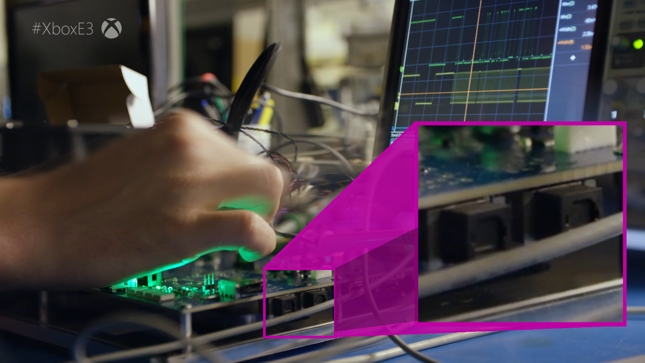
While going back through the Scarlett reveal trailer for other reasons, I noticed something in one of the motherboard shots. There seem to be two optical audio ports on this board:

spdifkgjga.png


This seems weird to me. Are these ports also for connections besides optical audio? Or would a devkit potentially have multiple audio jacks for some reason? Or what could they be for? Maybe there's an obvious answer and I'm just not getting it.
 

thebishop

Banned
Nov 10, 2017
2,758
While going back through the Scarlett reveal trailer for other reasons, I noticed something in one of the motherboard shots. There seem to be two optical audio ports on this board:

spdifkgjga.png


This seems weird to me. Are these ports also for connections besides optical audio? Or would a devkit potentially have multiple audio jacks for some reason? Or what could they be for? Maybe there's an obvious answer and I'm just not getting it.

One of them is Optical *IN*. Scarlett will control your minidisc player. The old MS is back baby!
 

vivftp

Member
Oct 29, 2017
19,744
John Sell, the guy who just left to go work for Intel.

The head architect for Scarlett left over a year out from launch? Is this just a case of him wanting to move on or is it normal for the head architect to no longer be needed at this stage of a consoles development when pretty much everything is locked in?
 

El-Pistolero

Banned
Jan 4, 2018
1,308
I'm gonna bow out until things cool down. Earlier in the thread, it felt like there was a good discussion but it's starting to feel a lot more heated right now, with lines being drawn and things taken out of context which is not something I want to get in the middle of again.

You and I are actually making the same points. There are plenty of reasons Cerny may not have been clear, and at no point did I accuse him of anything untoward. I'm not being naive or disingenuous. You're totally right - maybe he assumed it would be taken the way he meant it, maybe he was intending to set expectations, maybe he wanted to encourage the speculation. I dunno, but I totally agree with you. I'm not questioning his integrity.

I believe the PS5 will have HW RT.

You do not have to justify yourself, let alone excuse yourself from contributing to this thread on account og virtual warriors, whose worth seems to correlate with the performance level of an entertainement device. Many of us here appreciate your thoughtful posts, and I can write this with confidence. Plus you have a fantastic avatar, sir.
 

Gay Bowser

Member
Oct 30, 2017
17,645
Another cool previous fact: the PS3 shipped with a 395w power supply and had games go over 200W during gameplay. PS4 topped out at 150w during gameplay. If Sony is going for $499, why cant they have another 200w console?

I really don't think Sony is looking at the PS3 as a positive example.

More like a, "let's never do this again" kind of example.

I think the PS3 was also more power-hungry than initially intended, which is why the console grew between E3 2005 and 2006 (and gained tons of vents). Even in their Krazy Ken era, I don't think they set out to make a console that went over 200W during gameplay.
 
Liabe Brave's Project Scarlet Memory Configuration Speculation

Liabe Brave

Professionally Enhanced
Member
Oct 27, 2017
1,672
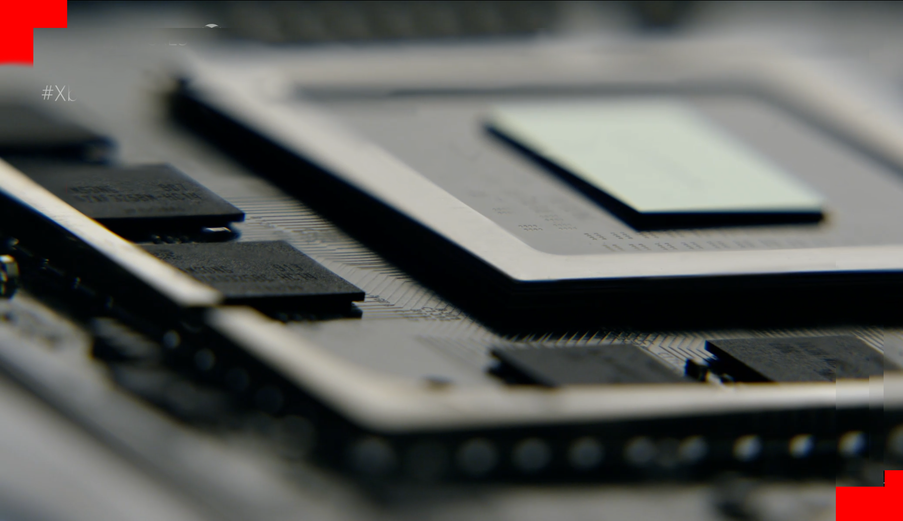
Here's the actual reason I was going through the Scarlett announce video again. I captured the very short sequence panning over the APU package area. There's a focus pull during this shot, so as it goes different parts of the image are in focus. I used multiple frames to paste together a version combining all parts while they're most clear. Here's the combined shot.

anapasteupq2jxq.png


There's no paint-in here--that is, I didn't add any pixels. But obviously, I made choices about where and what to erase and combine, and my decisions may not have preserved accuracy. This image should definitely not be relied on for size measurement, counting of traces, etc.

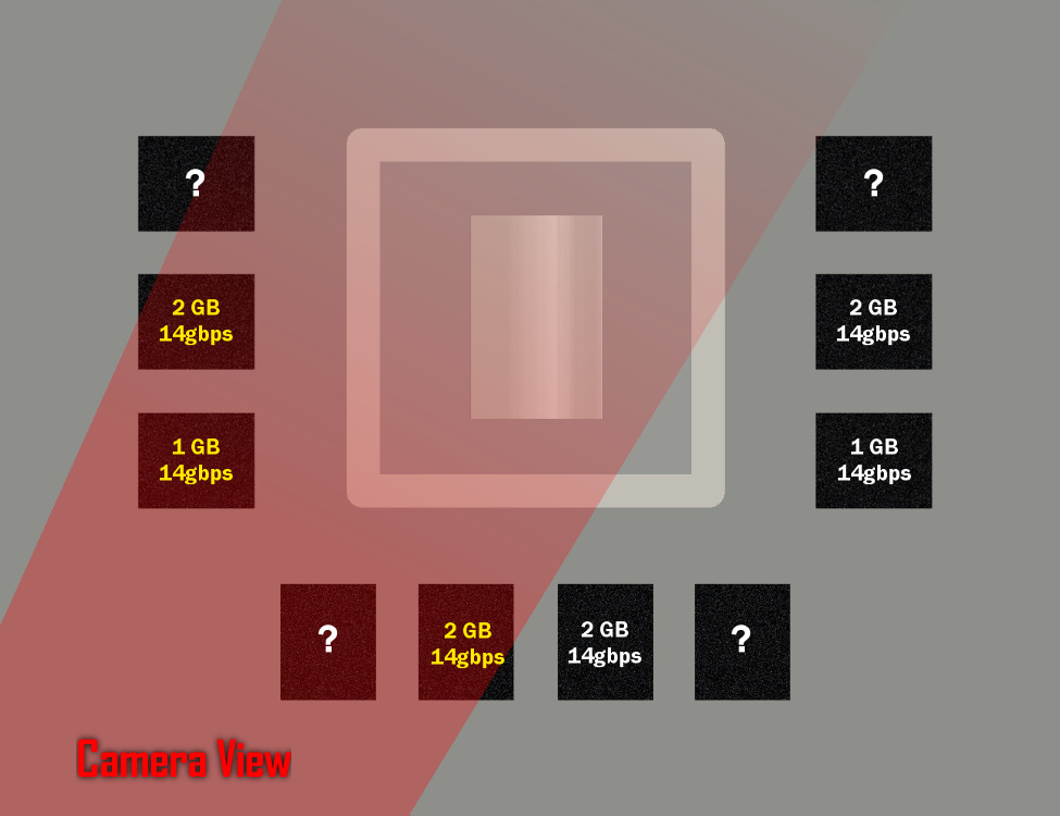
But it's good for rough conclusions, and I think well demonstrates the evidence for a 320-bit memory interface. There are apparently no RAM chips on the far side, so all would be situated to the left, bottom, and (offscreen) the right of the APU package. The 3 chips on the left fit entirely within the length of the package. The 2 chips at the bottom start outside the package edge, and don't reach the center of the die. It would thus make most sense for there to be 4 chips total at bottom, with 2 offscreen. Logically, there'd then be another 3 chips on the right. Though they can't be seen, the view past the top-right package corner shows no RAM in a corner position...and further down at the very edge, there's a mild dark blur that could be out-of-focus RAM in the expected position.

This adds up to very good evidence for 10 RAM chips in a 3-4-3 configuration. At 32-bit per GDDR6 chip, that's a 320-bit bus. Given 14bps chips (see below), total RAM bandwidth would be 560GB/s. That's about 72% higher than Xbox One X. It's 25% higher than both the new Navi GPUs and the Nvidia RTX 2080, though in Anaconda this would be shared with the CPU. (Note that this is a max figure for these particular GDDR6 chips. In One X, Microsoft downclocked the RAM slightly, so a repeat of that would give lower results.)

As for size, two different Samsung designations can be seen. The middle chip on the left, and probably the right one at bottom, are code 325BM-HC14. This is 16Gb/2GB capacity and 14Gbps speed. The lower chip on the left is code 325BC-HC14, an 8Gb/1GB capacity at the same speed. Presuming symmetry of the left with the proposed unseen chips on the right, we have 10GB known, plus 4 unknown chips. That'd allow 14, 16, or 18GB total.

Here's a rough overhead schematic showing the situation I described. The RAM labeled in yellow is definite, as we can read the part numbers. The RAM labeled in white is from assumption of symmetry. The remaining chips are unknown, and could be 1 or 2GB each.

anaoverheadsejik.jpg


Hopefully this is helpful for folks that hadn't seen this data fully explicated before. Note that apart from the newly enhanced image, none of this analysis is new from me. It was developed by others earlier, notably DukeBlueBall . But I believe a thorough layout like this will show that the memory bandwidth and (in a tight range) amount are probably known for Anaconda, even though not verbally announced by Microsoft.
 
Last edited:

DukeBlueBall

Banned
Oct 27, 2017
9,059
Seattle, WA
Here's the actual reason I was going through the Scarlett announce video again. I captured the very short sequence panning over the APU package area. There's a focus pull during this shot, so as it goes different parts of the image are in focus. I used multiple frames to paste together a version combining all parts while they're most clear. Here's the combined shot.

anapasteupq2jxq.png


This adds up to very good evidence for 10 RAM chips in a 3-4-3 configuration. At 32-bit per GDDR6 chip, that's a 320-bit bus. Given 14bps chips (see below), total RAM bandwidth would be 448GB/s. That's about 37% higher than Xbox One X; it's equal to both the new Navi GPUs and the Nvidia RTX 2080 (though in Anaconda this would be shared with the CPU).

One correction total ram bandwidth should be 560 GB/s.
 

Fafalada

Member
Oct 27, 2017
3,065
I mean sure but you're saying that without any testing
During development software is tested on 100s of machines, often in conditions worse than end user product(torture tests, flat out broken builds etc). The first thing that would happen in case of frame variance between machines that should perform the same would be sending bug-reports (and eventually return hw) to the platform holder.
 

AegonSnake

Banned
Oct 25, 2017
9,566
Of course it does. Have you seen what you quoted from my post ?
Your logic is that RX 5700 XT is too small of a GPU to reach a bigger die size for the SoC. Despite a 212mm2 GPU base, PS4 die size reaches 350mm2. And I doubt Jaguar is bigger than Zen 2 despite the process node difference.

Xbox One X ? 360mm2. Despite a 232mm2 GPU base.

This is what it has to do. Your claim is that RX 5700 with its 40CUs is too small to fit in such a big die size. The reality shows it wasnt a problem before.
i see what you are saying now. ive been under the assumption that zen 2 would take 70mm2. ive been adding it straight to the 5700xt die size.

i guess if we take the x1x or base ps4 examples, we are looking at roughly 120mm2 for the cpu alone? isnt it possible that the jaguars simply took up more space than the zen 2s would?

or are you assuming that the zen 2 would take up 100-120mm2 as well when you add it to the apu? if thats the case then the nav 10 makes sense for a 380mm2 scarlet.
 

Deleted member 1589

User requested account closure
Banned
Oct 25, 2017
8,576
The head architect for Scarlett left over a year out from launch? Is this just a case of him wanting to move on or is it normal for the head architect to no longer be needed at this stage of a consoles development when pretty much everything is locked in?
Yeah, I think so. Cerny mentioned that any substantial changes would result in a 6 months delay while developing consoles so I think both corporations wont take the risk.
 

vivftp

Member
Oct 29, 2017
19,744
Yeah, I think so. Cerny mentioned that any substantial changes would result in a 6 months delay while developing consoles so I think both corporations wont take the risk.

Yeah, I wasn't too sure what to make of that since my only knowledge about a "head architect" comes from Cerny and it looks like he'll be with Sony forever. It just sounded odd that such a key person would be gone when we're still over a year away from the next gen launching.
 

Erimriv

Member
Oct 30, 2017
107
So these Zen 2 cpu's for the next gen will be comparable in performance to what: a current ryzen 5 2600, ryzen 7?
 

Rylen

Member
Feb 5, 2019
462
AMD has been talking about Navi being built specifically for consoles in collaboration with Sony for over a year now haven't they?

I can't imagine AMD would spoil the PS5 release by showing everyone Sony's hand a year early.

And I can't imagine Sony would be very happy if the 5700 XT was basically the GPU in PS5, and AMD stole their thunder a year early.
 
Status
Not open for further replies.