Thx but it's different interview. The one I quoted was for DualShockers.
-
Ever wanted an RSS feed of all your favorite gaming news sites? Go check out our new Gaming Headlines feed! Read more about it here.
Next-gen PS5 and next Xbox speculation launch thread |OT6| - Mostly Fan Noise and Hot Air
- Thread starter Mecha Meister
- Start date
You are using an out of date browser. It may not display this or other websites correctly.
You should upgrade or use an alternative browser.
You should upgrade or use an alternative browser.
- Status
- Not open for further replies.
Threadmarks
View all 8 threadmarks
Reader mode
Reader mode
Recent threadmarks
Colbert's Next Gen Predictions Colbert's HDD vs SSD vs NVME Speed Comparison: Part 3 Kleegamefan's industry roots verified by ZhugeEX PlayStation 5 Dev Kit Image from Patent PlayStation 5 Dev Kit Drawings Kleegamefan - Next Generation Console Information DualShock 5 Patent Vote for the next OT titleWith costs of production increasing exponentially as we go to smaller nodes, i wouldnt be surprised if sony went with a smaller chip to save some money. though i dont know how much money they would be saving with a 320mm2 gpu compared to a 380mm2 gpu.
all i know is thats very risky. sony would be giving up precious CUs in favor of a hail mary on ridiculously high clockspeeds that might not have transpired if everything didnt go according to plan.
Expect game enviornments to look photorealistic thanks to megatextures used in the Rebirth video, at least in first party games, and character models to look very CGi. not everything can be photorealistic just yet, so expect stylized graphics like in the heretic demo, but i suspect some open world games set in barren lands will come very close to the rebirth video.
i thought the sony leaks showed that HBM2 would either stack on top of the APU or right around it. and a massive cooler would sit on top of it cooling everything from the APU to the HMB2 stacks.
Fake Edit: Found it.
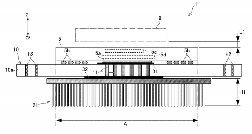
This post says it would go under the APU. Like how?
There's holes in the PCB through which metal posts or thermal paste create a thermal path to heatsink on the other side.
User Warned - Ableist Language
And again he told first-generation title... Currently all the graphics pipeline is not raytracing friendly. For example, all current shaders systems with tons of different shaders need to be redone for keeping only a few gloabl shaders because it kills intruction cache simply the worst cache miss existing... After there is some improvement they maybe have like LOD management for the BVH or data structure or ray reordering which aren't inside the first DXR implementation...
It is not meaning after some optimization and improvement you will not have some1440p title...
My analysis no studio will go 8k because this is too costly. This is 16x more than PS4...
Even mentioning 8k as a possible rez' target is just plain retard...
does that patent necessitates the usage of HBM? isnt it possible that they just covered their bases in that patent in case that a pro console will use one? or maybe that they were still unsure back at the creation of this patent whether they will use HBM in the final product?
Even mentioning 8k as a possible rez' target is just plain retard...
Yes wait GDC or SIGGRAPH presentation about next-gen console to know what will be the focus of games developer years 1 or 2... When they will think about real next gen title...
As an Xbox primary guy my expectations are tempered based on their constant messaging around frame rates and loading times. Obviously you need much more GPU to push 4K60 than 4K30 but none of the messaging currently boasts about elevating visual fidelity. I'm expecting 10 TF Navi and not falling for the 12-14 trap some are boasting about.
As an Xbox primary guy that loves cool graphics and 4K on my Xbox One X, the consistent words from Phil Spencer about frame rates and smooth gameplay are music to my ears. Gameplay is king for me, and I am excited to hear that be a design goal for them.
So I am guessing 21 is the heatsink.There's holes in the PCB through which metal posts or thermal paste create a thermal path to heatsink on the other side.
32 is the APU and 31 is the RAM module. 11 connects the APU to GPU. And in the final console build, you essentially flip this diagram upside down and the heatsink (21) goes on top with the APU in the middle and the RAM underneath it? Do i have this right?
The question is why? MS has RAM modules on the side. they dont need to be cooled, right? or at least the system fan will dissipate any heat generating from those modules since they are so far apart. So why would Sony go with this? Is HBM2 really that power efficient that it can be cooled with whatever is left over from the APU? This would help them with a smaller mobo and more space for SSD chips soldered on the mobo i guess.
I shouldn't respond couse you didn't deserve but it's you lucky day. Nope, I expect big improvement in graphics quality but not heavy rt (I pressume nextgen consoles will be less capable in this field than rtx2070).
Thank you for so graciously replying to me. RTX2070 (and even 2080) are already having trouble with RT on current-gen games that output higher than 1080p, and that's not even full scene RT, just reflections, etc. Why would you expect budget constrained machines to somehow output a higher Rez than 1080p with next-gen games using RT?
I don't think anyone expects the RT solution in consoles to be better then the RTX cards, but it's already impressive that it seems like we'll be getting RT games next gen. I expect to be given a choice of 4K/30 or 60 without RT and 1080p/30 with RT on next gen games.
So it seems you took to your mind what David Cage said :)I don't think anyone expects the RT solution in consoles to be better then the RTX cards, but it's already impressive that it seems like we'll be getting RT games next gen. I expect to be given a choice of 4K/30 or 60 without RT and 1080p/30 with RT on next gen games.
31/32 is a thermal interface to the mechanical package or heatsink assemblies.So I am guessing 21 is the heatsink.
32 is the APU and 31 is the RAM module. 11 connects the APU to GPU. And in the final console build, you essentially flip this diagram upside down and the heatsink (21) goes on top with the APU in the middle and the RAM underneath it? Do i have this right?
The question is why? MS has RAM modules on the side. they dont need to be cooled, right? or at least the system fan will dissipate any heat generating from those modules since they are so far apart. So why would Sony go with this? Is HBM2 really that power efficient that it can be cooled with whatever is left over from the APU? This would help them with a smaller mobo and more space for SSD chips soldered on the mobo i guess.
The purposes of this include moving the heatsink to the other side for EMI reasons (antenna on top-side can be affected by heatsink). It also helps get more effective thermal mass to remove heat if you have a heatsink on both sides.
In many applications, a large amount of heat is removed from the part through the PCB and it's copper mass. That's why this approach can be successful.
i hope some devs will just patch their dynamic res games to remove the upper limit of the resolution scaler.
Then the game will render above the TVs native resolution, your TV will scale the output frame to fit and you've kinda benefitted very little.
Unless, you also want to supersample any frames above native res? I don't even know if you can.
It's funny because I was under the impression that wide and slow was the best option for consoles, because you got the best performance per watt. I know a bigger die is more expensive, but still.
Generally yeah, but if wafer costs are indeed double what they were at the launch of PS4, then a larger die can mean ridiculously expensive silicon at launch.
They already came to that conclusion several years ago when designing the Xbox One X.
I expect them to have similar design principles on Scarlett as was seen on Scorpio, though perhaps some of their priorities changed given the hint of the die size. Prior to the Gonzalo and now Oberon leaks, I would've guessed Scarlett featured the higher clocks, but now I just can't seem to see how they could push 1800-2000 MHz and have an SOC around 380mm^2 in a console for a reasonable price - so something has to give, and my guess is they'll be clocked lower than the PS5.
I don't really trust the die size estimates based off the E3 Scarlett render at all. They're predicated on a shakey assumption that the Processor cover and RAM chips are to scale. The askew perspective also introduces additional opportunity for error.
I'd argue the estimates are looking at a level of accuracy to 1 significant figure. Not something I would put any confidence in myself.
Wide and slow is best when considering TDP. If you can figure out a way t cool the system though then smaller and faster is better.
Cooling itself is not the problem. The cost impact of the more potent cooling solution is the issue.
It's a cost issue fundamentally.
So what exactly is it that you're complaining about lol? From your posts it seemed like you were expecting next-gen consoles to have some secret NASA RT tech that let them output next-gen games with higher pixel count than current gen games with RT..
My analysis no studio will go 8k because this is too costly. This is 16x more than PS4...
8k support will be there for video and maybe the odd indie title(maybe). even 4k is going to be pushing it depending on game. if you look a the history of this gen and how the 1080p/60 dream eroded over the years, expect the same next gen with 4k.
Nope, I didn't expect at all rt in nextgen consoles and I'm not complaining.So what exactly is it that you're complaining about lol? From your posts it seemed like you were expecting next-gen consoles to have some secret NASA RT tech that let them output next-gen games with higher pixel count than current gen games with RT..
No hail mary's here. Its a very sound approach. Assume power consumption is equal, then you have two options. You either go wide but clock lower to stay withing target power draw and you wouldn't have to worry too much about TDP. Or you narrow and clock high (while using the same amount of power consumption) but will generate more heat which means you would have to deal with TDP better. No hail marys there and nothing is being given up. Just two different ways to arrive at the same solution. Then there is the added benefit that a smaller chip will cost less to make. Though the argument there can be that you then spend more on cooling.With costs of production increasing exponentially as we go to smaller nodes, i wouldnt be surprised if sony went with a smaller chip to save some money. though i dont know how much money they would be saving with a 320mm2 gpu compared to a 380mm2 gpu.
all i know is thats very risky. sony would be giving up precious CUs in favor of a hail mary on ridiculously high clockspeeds that might not have transpired if everything didnt go according to plan.
This post says it would go under the APU. Like how?
Yes, sony's patent basically suggests an APU cooling sandwich. If taking it literally. As it stans chips are cooled on one side of the PCB, sony is suggesting that cooling will happen on both sides. This could improve cooling efficiency by as much as 40-80% if cooling on the alternate side is half as god as cooling on the primary side of the PCB.
Stuff like that seems to be a common misconception around here. There is not a chance in hell that sony goes with a 36CU GPU while as far as they are concerned are pushing the envelope of console design, then MS, releasing in the same year, using the same architecture, and even the same general design layout comes and manages to put 48CU in a similarly priced and sized box. That is just flat out impossible.So if PS5 is going with Navi 10 Lite. What will MS use? Will they go with 48 CU or higher?
Just look at the PS4pro and XB1X. Both based on the Polaris architecture, and even releasing a year apart MS only managed to up the CU count by 4CU. And yet people expect them to up CU count by 12CU when releasing in the same year or even month? How?
Best I see MS doing is gong with a 40CU GPU (4CU with 4 deactivated) which would be a Navi 10 "full"
Last edited:
So if PS5 is going with Navi 10 Lite. What will MS use? Will they go with 48 CU or higher?
Navi 22 LIT*
*LIT = literally "lit", bitches!
Can we please drop 1080p once and for all (apart from games using RT ofc) and force developers (okay maybe not force) for next gen to use 4k native with 30 fps or 60. Just like we did with 720p this gen when those games were laughed at when they released. Only a few titles in the beginning of this gen used 720p from what I recall.
Nope, I didn't expect at all rt in nextgen consoles and I'm not complaining.
Got it, my bad. Seems like I read your posts wrong then lol.
It will certainly be interesting to see how both MS and Sony implement RT hardware into their respective console. For the record, I expect MS to use AMD's solution while Sony uses something else.
Why we expect 399$ if 9.2tf ? It's performance teritory of 5700xt which cost 399$ Ps4 that cost 399$ have gpu on 7850 performance level and launch price of 7850 was 249$. I still asume 499$ for ps5.
The 7870 was $350, the ps4 gpu was more powerful then a 7850 but less then a a 7870
I think the 8k support was more about video and a confirmation that this is a 2.1 HDMI hardware.8k support will be there for video and maybe the odd indie title(maybe). even 4k is going to be pushing it depending on game. if you look a the history of this gen and how the 1080p/60 dream eroded over the years, expect the same next gen with 4k.
When 8K TV will be more accessible, it will be the reason to exist for PS5 pro.
I prefer next gen to focus on 60 FPS and checkerboard over native 4k.
As an Xbox primary guy that loves cool graphics and 4K on my Xbox One X, the consistent words from Phil Spencer about frame rates and smooth gameplay are music to my ears. Gameplay is king for me, and I am excited to hear that be a design goal for them.
Just be prepared for the next gen GIF/Photomode comparisons as folks continue to battle graphics in 30FPS and 60FPS games. Linear vs. open world, etc. Prepare yourself.

I don't think we have nearly enough info to make truly informed guesses. I think they'll be roughly the same if priced similarly, any advantage being mostly inconsequential. But then again, I'm pretty sure Sony is going with $399, so if you think MS is going with $499, I guess I'd have them take the power crown.
though i dont know how much money they would be saving with a 320mm2 gpu compared to a 380mm2 gpu.
Kinda depends on defect density and a bunch of other stuff, but assuming averages for a fairly new process, you're talking about the bigger chip costing upwards of 30% more (and having considerably lower production volume, as well). So, if the small APU costs $90, big one would end up $120+.
No hail mary's here. Its a very sound approach. Assume power consumption is equal, then you have two options. You either go wide but clock lower to stay withing target power draw and you wouldn't have to worry too much about TDP. Or you narrow and clock high (while using the same amount of power consumption) but will generate more heat which means you would have to deal with TDP better. No hail marys there and nothing is being given up. Just two different ways to arrive at the same solution. Then there is the added benefit that a smaller chip will cost less to make. Though the argument there can be that you then spend more on cooling.
Yes, sony's patent basically suggests an APU cooling sandwich. If taking it literally. As it stans chips are cooled on one side of the PCB, sony is suggesting that cooling will happen on both sides. This could improve cooling efficiency by as much as 40-80% if cooling on the alternate side is half as god as cooling on the primary side of the PCB.
Lets compare PS4 Pro with Xbox 1X:
Same GPU uarch family (broadly):
Pro Clocks 911 MHz
X1X Clock 1172 MHz
X1X is 29% higher clocks.
PS4 Pro peak power consumption is around 175W.
X1X peak averages between 180W to 200W.
29% higher power consumption than 175W is 225W and afaict the X1X doesn't go that high.
Now recall, X1X also has more GDDR5 chips AND roughly 10% more CUs... so expected peak power should have been greater than 225W for the X1X.... but it isn't.
So I guess there's more to it than just die size and clocks. You have to consider the entire system design and at least with the Pro and X1X MS was certainly doing something that Sony wasn't.
So I guess there's more to it than just die size and clocks. You have to consider the entire system design and at least with the Pro and X1X MS was certainly doing something that Sony wasn't.
One thing to keep in mind is that die size isn't just CUs. Pro CUs we're slightly bigger and did more stuff than Xs. Another thing to keep in mind is that we don't know how much power the Pro APU was wasting, on average, pushing unnecessary voltage to guarantee yields - we know that the X wasn't using any.
Green Team resigning themselves to a narrower, higher clocked design it seems.
So is it going to be 60 or 66 active CUs for Scarlett?
I'm leaning towards 60 active but ymmv.
So is it going to be 60 or 66 active CUs for Scarlett?
I'm leaning towards 60 active but ymmv.
1.84tf is very close to 1.76tf and far from 2.56tfThe 7870 was $350, the ps4 gpu was more powerful then a 7850 but less then a a 7870
One thing to keep in mind is that die size isn't just CUs. Pro CUs we're slightly bigger and did more stuff than Xs. Another thing to keep in mind is that we don't know how much power the Pro APU was wasting, on average, pushing unnecessary voltage to guarantee yields - we know that the X wasn't using any.
In theory, assuming Sony wasn't observing something like the Hovis method, their chips should actually clock stabler at lower voltages---unless they really pushed the boat out in order to maximise yields.
Regardless, this is precisely the point I was driving at. The manufacturing process has possibly more of an impact on the relationship between clocks and perf/watt for the average chip. So if you're only focussed on die size and clocks, you're not seeing the full picture.
Also, I doubt RPM makes much difference to the Pros CUs at all. If you compare the ratio of Pro die size to the X1X die size and then compare with the ratio of CU counts it broadly aligns.
Green Team resigning themselves to a narrower, higher clocked design it seems.
So is it going to be 60 or 66 active CUs for Scarlett?
I'm leaning towards 60 active but ymmv.
Curious... how is this narrower?
But they used the chip in the 7870, disabled two CUs and lowered the clocks by 200 mhz. 7850 only had 16 CUs.
Had they gone with a better cooling solution, they couldve clocked it at 1000 mhz and hit 2.3 tflops with the same chip. If MS hadnt gone with a shit 1.2 tflops GPU, sony would've at least thought about clocking it higher to get the advantage.
Thats exactly what they seem to be doing now. Both MS and Sony seem to want the power advantage. And the only winner is going to be us the consumer.
Fair point but as you see, 399$ > 349$ + more expensive cooling system for this very high clocks on ps5.But they used the chip in the 7870, disabled two CUs and lowered the clocks by 200 mhz. 7850 only had 16 CUs.
Had they gone with a better cooling solution, they couldve clocked it at 1000 mhz and hit 2.3 tflops with the same chip. If MS hadnt gone with a shit 1.2 tflops GPU, sony would've at least thought about clocking it higher to get the advantage.
Thats exactly what they seem to be doing now. Both MS and Sony seem to want the power advantage. And the only winner is going to be us the consumer.
Cerny - "Challenge accepted"HBM + 2GHz GPU + 8 core zen 2 all chugging away in the same spot is going to be really challenging from a thermal/cooling perspective
It's going to be 36-40 on both I think.Green Team resigning themselves to a narrower, higher clocked design it seems.
So is it going to be 60 or 66 active CUs for Scarlett?
I'm leaning towards 60 active but ymmv.
which is why i think they went with a wide and slow approach initially and have only now begun to push clocks because they can. the first gonzolo leak was 1ghz. Do we really believe that was a 36 CU chip?Fair point but as you see, 399$ > 349$ + more expensive cooling system for this very high clocks on ps5.
i do think an expensive cooling system was always part of their design. If they knew in 2015 they wanted an SSD, they wouldve known that a $399 console was out of the picture. With an extra $100 to play with, a bigger APU and a more expensive cooling system to hit those high clocks is definitely on the cards.
Can we please drop 1080p once and for all (apart from games using RT ofc) and force developers (okay maybe not force) for next gen to use 4k native with 30 fps or 60. Just like we did with 720p this gen when those games were laughed at when they released. Only a few titles in the beginning of this gen used 720p from what I recall.
Hate to break it to you but many games are still running at sub 1080p this gen.
I'll take 1080p with raytracing any day over 4K.
You will no get 2ghz console gpu with more than 36cu. 1ghz for first engeneering gonzalo sample seems quite reasonable.which is why i think they went with a wide and slow approach initially and have only now begun to push clocks because they can. the first gonzolo leak was 1ghz. Do we really believe that was a 36 CU chip?
i do think an expensive cooling system was always part of their design. If they knew in 2015 they wanted an SSD, they wouldve known that a $399 console was out of the picture. With an extra $100 to play with, a bigger APU and a more expensive cooling system to hit those high clocks is definitely on the cards.
You will no get 2ghz console gpu with more than 36cu. 1ghz for first engeneering gonzalo sample seems quite reasonable.
1ghz is not reasonable. I'm assuming that was an engineering sample.
- PS5 - 72 @ 1550
- Scarlett - 60 @ ~1700
Sorry, my mistake. Always thought ps4 was closer to the 7870 for some reason.
Yes, MS was using a vapor chamber cooling solution.Lets compare PS4 Pro with Xbox 1X:
Same GPU uarch family (broadly):
Pro Clocks 911 MHz
X1X Clock 1172 MHz
X1X is 29% higher clocks.
PS4 Pro peak power consumption is around 175W.
X1X peak averages between 180W to 200W.
29% higher power consumption than 175W is 225W and afaict the X1X doesn't go that high.
Now recall, X1X also has more GDDR5 chips AND roughly 10% more CUs... so expected peak power should have been greater than 225W for the X1X.... but it isn't.
So I guess there's more to it than just die size and clocks. You have to consider the entire system design and at least with the Pro and X1X MS was certainly doing something that Sony wasn't.
And yes, the entire system needs to be considered. But when talking about GPU power, it literally boils down to clocks and TDP. You clock higher than you are"supposed to" and you will run into TD issues for which you will need to use better cooling. You go bigger than you are supposed to then you will run into power consumption issues for which you will need to clock lower.
What we can't know is what is big enough or what is fast enough, cause as long as you are working within those limits you are fine.
Now looking at the 5700xt, its clear where those limits are. So if sony wants to clock higher then there are only two ways that is possible and maybe even a combination of both. Using a better or more efficient manufacturing process (7nm+) or using significantly more advanced cooling. If MS is opting to go wider then that would also mean that they would be set on working within the thermal limits of the current arch which again thanks to 5700xt we also know. So they can gain performance by not having to push much harder than the stock 5700xt which remember is also using a vapor chamber cooler.
Yes, MS was using a vapor chamber cooling solution.
And yes, the entire system needs to be considered. But when talking about GPU power, it literally boils down to clocks and TDP. You clock higher than you are"supposed to" and you will run into TD issues for which you will need to use better cooling. You go bigger than you are supposed to then you will run into power consumption issues for which you will need to clock lower.
What we can't know is what is big enough or what is fast enough, cause as long as you are working within those limits you are fine.
Now looking at the 5700xt, its clear where those limits are. So if sony wants to clock higher then there are only two ways that is possible and maybe even a combination of both. Using a better or more efficient manufacturing process (7nm+) or using significantly more advanced cooling. If MS is opting to go wider then that would also mean that they would be set on working within the thermal limits of the current arch which again thanks to 5700xt we also know. So they can gain performance by not having to push much harder than the stock 5700xt which remember is also using a vapor chamber cooler.
TDP is thermal design power. I'm talking about electrical power consumption.
Vapour chamber or any other cooling method doesn't magically change how much power a chip consumes.
You've got it wrong.
The important factors are:
- Transistor count (of which die size is a proxy for)
- Clock speed
- Voltage
It's even more complicated than that but it gives you a good guide.
PS5 could also mark the return of tiered console launches. But I think the lower priced one will be 399 with a 1 tb ssd and the higher priced 499 with 2.5 tb ssd.
Neither will be user replaceable.
Yup, I mentioned it before, the smartphone model. $100 for an extra 1TB of memory would be a great deal, actually, Apple charges something like $200 to go from 256GB to 512GB. Price premium on the higher tier could offset any losses into profitability.
EDIT: wouldn't surprise me much if the tiers were 512GB and 1TB for $399 and $499 respectively, too.
Last edited:
People also said you'd never get 1.8 clock, let alone 2. Yet here we areYou will no get 2ghz console gpu with more than 36cu. 1ghz for first engeneering gonzalo sample seems quite reasonable.
This might be Sonys checkerboard rendering for Ray tracing.Komachi mentioned RayTracing only for Arden.
That could mean Ray tracing being hardware only on Scarlett and not PS5. Or Scarlet could have more hardware dedicated to RT, while PS5 only some minor stuff, like the AMD TMU (textures unit) patent.
Because it's sub 10tflops, and only 16GB of memory. But I think they'll lose more money for each console sold compard to PS4.
But that's a voxel based global illumination method, the name itself implies that. Sure, you could argue that it's tracing rays to a degree, but that's through a voxelized representation of the scene not actually casting rays and tracing them in each pixel in a scene comprised of geometry.Yes, and that's always been a raytracer, capable of reflections and all.
Threadmarks
View all 8 threadmarks
Reader mode
Reader mode
Recent threadmarks
Colbert's Next Gen Predictions Colbert's HDD vs SSD vs NVME Speed Comparison: Part 3 Kleegamefan's industry roots verified by ZhugeEX PlayStation 5 Dev Kit Image from Patent PlayStation 5 Dev Kit Drawings Kleegamefan - Next Generation Console Information DualShock 5 Patent Vote for the next OT title- Status
- Not open for further replies.