I think what's probably happening is that they're trying to ensure they have enough stock for something that's happening next week, likely some promo or something involving Zelda, based on the leaked poster.I just can't see why that would prompt Gamestop to stop selling the system. It's selling at a very brisk pace, why would they put a week-long pause on that? They can't really afford any frivolities like that I'd think. That's why the only slightly sensible explanation I can think of is that they fear getting stuck with a bunch of trade-in Switches because of the announcement of a Pro (but I'm not banking on that being the case, of course).
You are using an out of date browser. It may not display this or other websites correctly.
You should upgrade or use an alternative browser.
You should upgrade or use an alternative browser.
Threadmarks
View all 6 threadmarks
Reader mode
Reader mode
Recent threadmarks
Excellent explanation of how DLSS works. A short, detailed summary of why Ampere might be used rather than Turing in terms of DLSS. Mod message in regards to hostility to insiders and other members regarding OLED model Poll on who should create the 2nd OT thread Poll results update with added deadline Final poll resultsHm, maybe. I'm not convinced, but one possible thing they might do is to bundle the Switch with some software in order to increase per-sale revenue and profit (Switch + Link's Awakening/BOTW1 + poster for $400 or whatnot), assuming they believe they can sell every system they have not sold during the past week. I could maybe see that, but it also doesn't strike me as a master plan, either, tbh.I think what's probably happening is that they're trying to ensure they have enough stock for something that's happening next week, likely some promo or something involving Zelda, based on the leaked poster.
For sake of shifting discussion to something I think is more interesting (personally to help figure out), but what is the possible per SM power draw of Ampere?
I think the best possible comparisons or the ones to draw possible numbers are the 3070 and 3060TI, they have the same type of RAM (GDDR6), same amount (8GB) and it is the same clock (1750MHz), their SM count and their clocks are, however, different.
3070 has 46 SMs with a base clock of 1500MHz and a boost clock of 1725MHz. TFLOPS: ~20.
3060TI has 38 SMs with a base clock of 1410MHz and boost clock of 1665MHz. TFLOPS: ~16.
Reason is that, I think we can extrapolate from this for the switch, at least some information regarding it.
Even if they don't exactly scale linearly.
In general, it's pretty atypical for threads to get pinned to particular cores. Most multithreaded software just trusts the OS to make sane decisions when it comes to scheduling threads to CPU cores because it's generally going to have a clearer, more complete picture of what would be best for the system as a whole.
I'm pretty sure most games are not multithreaded, that's a high level of expertise that most devs don't have at all in several other fiields in games.
It also doesn't make sense to use threads in most games workloads. The OS, even an OS designed for game consoles, will never make a better decision than the game programmer who knows exactly what is needed where on a game console (a general usage computer like a PC or a smartphone is different).
So process affinity is used, but again only by the most proficient devs. Given the nature of threads, they will be pinned to specific cores too if the parent process is.
Process affinity is paramount to extract the best perf from the hardware with cache management and avoiding expensive process scheduling.
That said, game consoles are exactly the sort of fixed, highly controlled environment where thread pinning tends to show up, so there probably are a bunch of Switch games that do it. It's still enough of a micro-optimization that I'm not sure if it would really be the norm, though.
It's not thread pinning, these are not Windows-like OS but POSIX-like OS, it's process affinity. And it's not a micro-optimization at all, it's a high level optimization that will give the best results. I don't know if it has been theorized, but the best course of action is usually to use instrumentation and profiling to get the best course of action. But being a higher level programmer tech, ofc few game devs are able to use it. And I'm talking devs that use low-level coding languages.
Let's take the RTX3060Ti. It consumes "up to 200W", so let's calculate with that and the boost clock. Our target for the GPU power draw is 3W in handheld mode. Let's explore 2 possibilities: a 6SM GPU and a 4SM GPU.For sake of shifting discussion to something I think is more interesting (personally to help figure out), but what is the possible per SM power draw of Ampere?
I think the best possible comparisons or the ones to draw possible numbers are the 3070 and 3060TI, they have the same type of RAM (GDDR6), same amount (8GB) and it is the same clock (1750MHz), their SM count and their clocks are, however, different.
3070 has 46 SMs with a base clock of 1500MHz and a boost clock of 1725MHz. TFLOPS: ~20.
3060TI has 38 SMs with a base clock of 1410MHz and boost clock of 1665MHz. TFLOPS: ~16.
Reason is that, I think we can extrapolate from this for the switch, at least some information regarding it.
Even if they don't exactly scale linearly.
For 6SM, we reduce power draw by 38/6 -> 31.6W at 1665 MHz, for 2.53 TFLOPS. Using the squared frequency rule of thumb, we have to reduce the wattage by a factor 31.6/3 and therefore drop the frequency by sqrt(31.6/3), giving us 1665/sqrt(31.6/3) = 513 MHz, which represents a 0.78 TFLOPS GPU in handheld mode.
For 4SM, we reduce the power draw by 38/4 -> 21.05W at 1665 MHz, for 1.68 TFLOPS. We must reduce the wattage further by a factor 7, giving a frequency of 630 MHz, which represents a 0.64 TFLOPS GPU.
A good rule of thumb would be to double those numbers to get docked GPU performance, although you could probably get away with quite a bit more in docked mode if you wanted to. But yeah, we need to be careful assuming that these simple mathematical computation hold completely, since we don't have a guarantee things scale linearly (and quadratically) in this manner to a much smaller GPU. On the other hand, Switch might allow TDP to be slightly higher than 3W because it is not the average power draw (it is peak power draw). So I dunno, apply plenty of caveats, but the above is not necessarily unreasonable if we do get an Ampere GPU.
Edit: if we do the same for the RTX3070 (TDP=220W), we would get:
For 6SM, the wattage at 1725 MHz is 28.7W. We must drop frequency by sqrt(28.7/3) to 558 MHz, giving a 0.84 TFLOPS GPU in handheld mode.
For 4SM, the wattage at 1725 MHz is 19.1W. We must drop frequency by sqrt(19.1/3) to 683 MHz, giving a 0.69 (nice) TFLOPS GPU in handheld mode.
Edit 2: Let's also do it for the RTX3050, which has a TDP of 90W, a boost clock of 1740 MHz, 18 SMs, and a peak performance of 8 TFLOPS:
For 6 SM, we have a power draw of 30W at 1740 MHz. We must drop the frequency by sqrt(10) to 550 MHz, giving a 0.84 TFLOPS GPU in handheld mode.
For 4 SM, we have a power draw of 20W at 1740 MHz. We drop the frequency by sqrt(20/3) to 674 MHz, giving a 0.69 TFLOPS GPU in handheld mode.
This is a pretty interesting result, since it's in line with the RTX3070. No guarantees, of course, but it could lend some credence to the idea that the power consumption scales pretty linearly to lower SM counts.
Edit 3: Also, if this is based on Orin, then it'd lose the RT cores in favour of bigger Tensor cores, so it's hard to say whether the FLOPS number and power draw will remain unaffected by that
Last edited:
Yeah, I agree that neural nets can be a very viable middleground between exact simulation (computationally heavy) and hardcoded data (storage-heavy). Approximating differential equations with neural nets has been an active area of research in recent years, so I wonder if there are implementations in the gaming industry outside of Ubisoft's one as detailed in the blog post.What I understood from that part of the blog post was:
- Get something very hard to compute.
- Create a huge set of input-outputs.
- Train multiple ML algorithms with that set.
- Verify which ML algorithm uses the least resources while delivering satisfactory accuracy
- Ship the software with that ML algorithm, which will require far less computing than the original calculation, while being much smaller than hardcoding the innumerable possible input-output.
In your example, they don't need ML to compute how the dress will move in the next 1s, they can brute force it in their supercomputers. The problem is that they don't want to neither compute in real time nor hardcode the dress movement for every single possible movement the body could do (because it would use too much memory instead).
While not acurate, it gives us a ballpark that im more than happy with. 2-4 times the GPU power would be awesome.Let's take the RTX3060Ti. It consumes "up to 200W", so let's calculate with that and the boost clock. Our target for the GPU power draw is 3W in handheld mode. Let's explore 2 possibilities: a 6SM GPU and a 4SM GPU.
For 6SM, we reduce power draw by 38/6 -> 31.6W at 1665 MHz, for 2.53 TFLOPS. Using the squared frequency rule of thumb, we have to reduce the wattage by a factor 31.6/3 and therefore drop the frequency by sqrt(31.6/3), giving us 1665/sqrt(31.6/3) = 513 MHz, which represents a 0.78 TFLOPS GPU in handheld mode.
For 4SM, we reduce the power draw by 38/4 -> 21.05W at 1665 MHz, for 1.68 TFLOPS. We must reduce the wattage further by a factor 7, giving a frequency of 630 MHz, which represents a 0.64 TFLOPS GPU.
A good rule of thumb would be to double those numbers to get docked GPU performance, although you could probably get away with quite a bit more in docked mode if you wanted to. But yeah, we need to be careful assuming that these simple mathematical computation hold completely, since we don't have a guarantee things scale linearly (and quadratically) in this manner to a much smaller GPU. On the other hand, Switch might allow TDP to be slightly higher than 3W because it is not the average power draw (it is peak power draw). So I dunno, apply plenty of caveats, but the above is not necessarily unreasonable if we do get an Ampere GPU.
Edit: if we do the same for the RTX3070 (TDP=220W), we would get:
For 6SM, the wattage at 1725 MHz is 28.7W. We must drop frequency by sqrt(28.7/3) to 558 MHz, giving a 0.84 TFLOPS GPU in handheld mode.
For 4SM, the wattage at 1725 MHz is 19.1W. We must drop frequency by sqrt(19.1/3) to 683 MHz, giving a 0.69 (nice) TFLOPS GPU in handheld mode.
There are probably still a fair number of single-threaded games, but there's been over a decade of work getting games to better utilize mutli-core CPUs at this point. Most games are probably at least lightly threaded by now. It doesn't take a genius to write multi-threaded code, especially when your game engine is probably doing a fair amount of the work for you.I'm pretty sure most games are not multithreaded, that's a high level of expertise that most devs don't have at all in several other fiields in games.
It also doesn't make sense to use threads in most games workloads. The OS, even an OS designed for game consoles, will never make a better decision than the game programmer who knows exactly what is needed where on a game console (a general usage computer like a PC or a smartphone is different).
So process affinity is used, but again only by the most proficient devs. Given the nature of threads, they will be pinned to specific cores too if the parent process is.
Process affinity is paramount to extract the best perf from the hardware with cache management and avoiding expensive process scheduling.
It's not thread pinning, these are not Windows-like OS but POSIX-like OS, it's process affinity. And it's not a micro-optimization at all, it's a high level optimization that will give the best results. I don't know if it has been theorized, but the best course of action is usually to use instrumentation and profiling to get the best course of action. But being a higher level programmer tech, ofc few game devs are able to use it. And I'm talking devs that use low-level coding languages.
Trying to control what cores your threads are scheduled to is just generally not worth the effort unless you're in a very controlled environment where you have a known number cores to work with (which is true for consoles and sometimes servers, but not so much in general), and even then, it's usually not worth the effort unless you're not getting the results you want without doing it. This is why I'm referring to it as a micro-optimization, because it's a very targeted, low-level optimization that can potentially be used to speed up a critical code path. It probably shows up more on Switch than on other consoles, but only because of how many games get ported to it that need a lot of optimization because they were originally designed for stronger CPUs.
Also, call the technique whatever you want, but Sony is the only one of the big 3 that's using a POSIX OS. The Switch is running a kernel that appears to have been developed entirely in-house by Nintendo which is decidedly not POSIX. There was some initial misreporting that it ran BSD based on the license page, but that was only actually referring to some networking code.
I can tell you just from monitoring the CPU usage of various Switch games that this is false. Many games are capable of pegging one core in the high nineties while 1-2 more run above 50% utilization.I'm pretty sure most games are not multithreaded, that's a high level of expertise that most devs don't have at all in several other fiields in games.
Would this account the RAM as well in the TDP of the card? I specified that as the cards have the exact same in terms of memory. We know that from GDDR6 to GDDR6X it consumes 15% less power per bit transfer, but overall due to being much faster it consumes a lot more.Let's take the RTX3060Ti. It consumes "up to 200W", so let's calculate with that and the boost clock. Our target for the GPU power draw is 3W in handheld mode. Let's explore 2 possibilities: a 6SM GPU and a 4SM GPU.
For 6SM, we reduce power draw by 38/6 -> 31.6W at 1665 MHz, for 2.53 TFLOPS. Using the squared frequency rule of thumb, we have to reduce the wattage by a factor 31.6/3 and therefore drop the frequency by sqrt(31.6/3), giving us 1665/sqrt(31.6/3) = 513 MHz, which represents a 0.78 TFLOPS GPU in handheld mode.
For 4SM, we reduce the power draw by 38/4 -> 21.05W at 1665 MHz, for 1.68 TFLOPS. We must reduce the wattage further by a factor 7, giving a frequency of 630 MHz, which represents a 0.64 TFLOPS GPU.
A good rule of thumb would be to double those numbers to get docked GPU performance, although you could probably get away with quite a bit more in docked mode if you wanted to. But yeah, we need to be careful assuming that these simple mathematical computation hold completely, since we don't have a guarantee things scale linearly (and quadratically) in this manner to a much smaller GPU. On the other hand, Switch might allow TDP to be slightly higher than 3W because it is not the average power draw (it is peak power draw). So I dunno, apply plenty of caveats, but the above is not necessarily unreasonable if we do get an Ampere GPU.
Edit: if we do the same for the RTX3070 (TDP=220W), we would get:
For 6SM, the wattage at 1725 MHz is 28.7W. We must drop frequency by sqrt(28.7/3) to 558 MHz, giving a 0.84 TFLOPS GPU in handheld mode.
For 4SM, the wattage at 1725 MHz is 19.1W. We must drop frequency by sqrt(19.1/3) to 683 MHz, giving a 0.69 (nice) TFLOPS GPU in handheld mode.
Edit 2: Let's also do it for the RTX3050, which has a TDP of 90W, a boost clock of 1740 MHz, 18 SMs, and a peak performance of 8 TFLOPS:
For 6 SM, we have a power draw of 30W at 1740 MHz. We must drop the frequency by sqrt(10) to 550 MHz, giving a 0.84 TFLOPS GPU in handheld mode.
For 4 SM, we have a power draw of 20W at 1740 MHz. We drop the frequency by sqrt(20/3) to 674 MHz, giving a 0.69 TFLOPS GPU in handheld mode.
This is a pretty interesting result, since it's in line with the RTX3070. No guarantees, of course, but it could lend some credence to the idea that the power consumption scales pretty linearly to lower SM counts.
Taking into account the 2080 who has the same ram config, has a consumption of "up tp 175W"
and if we look here based on the results below:

There's more here if you were curious:
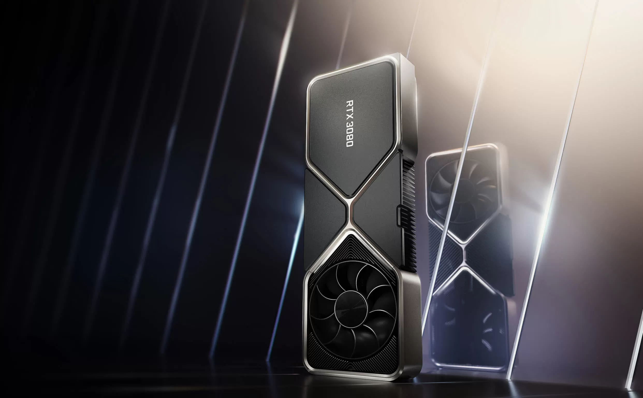
Nvidia GeForce RTX 3080 Review
Nvidia claims the new GeForce RTX 30 graphics series provides a giant leap in raw graphics performance, based their latest Ampere architecture, today we can finally show...
I also found the eurogamer chart to give interesting tidbits with regards to the 3070 even in comparison to the 2070:

Nvidia GeForce RTX 3070 review: welcome to the new mid-range
Digital Foundry review the Nvidia RTX 3070, the best value Ampere graphics card. Game benchmarks, hardware breakdown, power tests and more.
what I note is that, while the RAM is the same setup, the rest of it is not (clearly). The boost clock is different, uArch is different, the node is in fact different. Turing is less efficient than Ampere and that is a given. But the difficult part is piecing the RAM and how much it is accounted for, if at all, in the watts. Well, of course it is. lol
Last edited:
Considering the VRAM is part of the GPU chip, it has to be included in the TDP. So yeah, that would be another thing that would have to be subtracted from the RTX 30-cards in order to make the Switch comparison more equal.Would this account the RAM as well in the TDP of the card? I specified that as the cards have the exact same in terms of memory. We know that from GDDR6 to GDDR6X it consumes 15% less power per bit transfer, but overall due to being much faster it consumes a lot more.
Taking into account the 2080 who has the same ram config, has a consumption of "up tp 175W"
and if we look here based on the results below:
There's more here if you were curious:
Nvidia GeForce RTX 3080 Review
Nvidia claims the new GeForce RTX 30 graphics series provides a giant leap in raw graphics performance, based their latest Ampere architecture, today we can finally show...www.techspot.com
I also found the eurogamer chart to give interesting tidbits with regards to the 3070 even in comparison to the 2070:
Nvidia GeForce RTX 3070 review: welcome to the new mid-range
Digital Foundry review the Nvidia RTX 3070, the best value Ampere graphics card. Game benchmarks, hardware breakdown, power tests and more.www.eurogamer.net
what I note is that, while the RAM is the same setup, the rest of it is not (clearly). The boost clock is different, uArch is different, the node is in fact different. Turing is less efficient than Ampere and that is a given. But the difficult part is piecing the RAM and how much it is accounted for, if at all, in the watts. Well, of course it is. lol
I wouldn't be surprised if it's automotive chips or HPC chips on Intel's 7nm
I do find this interesting because it possibly shows the potential roadmap of manufacturing they may use going forward to meet the demand. Intel's 7nm process is expected to have a transistor density of 200-250Mtr/mm2(which is well above TSMC's 5nm process) so we may fully see something come about with this for the next-generation architecture from Nvidia.
Intel May Rename its 7nm Process Node to 5nm to Highlight Similarity w/ TSMC's 5nm EUV Process | Hardware Times
Intel is finally expected to make the shift to its 10nm node later this year in the volume market with Ice Lake-SP and Alder Lake-S after nearly six years of 14nm lineups. Although the naming convention dictates that the Intel 10nm node should be behind TSMC’s 7nm in terms of density...
Maybe some Zelda games preloaded on all switches sold after the direct or something. Stil weird to halt sales for that.This is such a weird rumour. Even if Nintendo plan to announce a Switch Pro, that wouldn't be a reason to halt OG Switch sales, right? Or would it be a Gamestop initiative in order to prevent the administrative work of many cancellations once the Pro has been announced?
Weird.
Let's take the RTX3060Ti. It consumes "up to 200W", so let's calculate with that and the boost clock. Our target for the GPU power draw is 3W in handheld mode. Let's explore 2 possibilities: a 6SM GPU and a 4SM GPU.
For 6SM, we reduce power draw by 38/6 -> 31.6W at 1665 MHz, for 2.53 TFLOPS. Using the squared frequency rule of thumb, we have to reduce the wattage by a factor 31.6/3 and therefore drop the frequency by sqrt(31.6/3), giving us 1665/sqrt(31.6/3) = 513 MHz, which represents a 0.78 TFLOPS GPU in handheld mode.
For 4SM, we reduce the power draw by 38/4 -> 21.05W at 1665 MHz, for 1.68 TFLOPS. We must reduce the wattage further by a factor 7, giving a frequency of 630 MHz, which represents a 0.64 TFLOPS GPU.
A good rule of thumb would be to double those numbers to get docked GPU performance, although you could probably get away with quite a bit more in docked mode if you wanted to. But yeah, we need to be careful assuming that these simple mathematical computation hold completely, since we don't have a guarantee things scale linearly (and quadratically) in this manner to a much smaller GPU. On the other hand, Switch might allow TDP to be slightly higher than 3W because it is not the average power draw (it is peak power draw). So I dunno, apply plenty of caveats, but the above is not necessarily unreasonable if we do get an Ampere GPU.
Edit: if we do the same for the RTX3070 (TDP=220W), we would get:
For 6SM, the wattage at 1725 MHz is 28.7W. We must drop frequency by sqrt(28.7/3) to 558 MHz, giving a 0.84 TFLOPS GPU in handheld mode.
For 4SM, the wattage at 1725 MHz is 19.1W. We must drop frequency by sqrt(19.1/3) to 683 MHz, giving a 0.69 (nice) TFLOPS GPU in handheld mode.
Edit 2: Let's also do it for the RTX3050, which has a TDP of 90W, a boost clock of 1740 MHz, 18 SMs, and a peak performance of 8 TFLOPS:
For 6 SM, we have a power draw of 30W at 1740 MHz. We must drop the frequency by sqrt(10) to 550 MHz, giving a 0.84 TFLOPS GPU in handheld mode.
For 4 SM, we have a power draw of 20W at 1740 MHz. We drop the frequency by sqrt(20/3) to 674 MHz, giving a 0.69 TFLOPS GPU in handheld mode.
This is a pretty interesting result, since it's in line with the RTX3070. No guarantees, of course, but it could lend some credence to the idea that the power consumption scales pretty linearly to lower SM counts.
Edit 3: Also, if this is based on Orin, then it'd lose the RT cores in favour of bigger Tensor cores, so it's hard to say whether the FLOPS number and power draw will remain unaffected by that
The mobile Ampere parts are probably a better reflection on where to estimate from since the efficiency definitely changes quite a bit with the lower clocked GPU's. You have to factor in what the RAM is drawing on these desktop cards in order to establish a good base for guesstimating.
Edit: just read that you replied to this already
Just for comparison though Nvidia lists the RTX 3050 laptop variant for 35 watts @ 1.057Ghz for a 16SM part, so a 6-8 SM GPU part should be able to achieve the desired performance metrics for 12 watts or less.
Last edited:
That's true. If we look at the RTX3070, the boost clock is 1560 MHz, 40 SMs, TDP=115W, and 16 TFLOPS:The mobile Ampere parts are probably a better reflection on where to estimate from since the efficiency definitely changes quite a bit with the lower clocked GPU's. You have to factor in what the RAM is drawing on these desktop cards in order to establish a good base for guesstimating.
Edit: just read that you replied to this already
Just for comparison though Nvidia lists the RTX 3050 laptop variant for 35 watts @ 1.057Ghz for a 16SM part, so a 6-8 SM GPU part should be able to achieve the desired performance metrics for 12 watts or less.
For 6SM, the power draw at 1560 MHz is 17.25W. That means the target frequency is 651 MHz, leading to 1.0 TFLOPS of GPU in handheld mode at 3W.
For 4SM, the power draw at 1560 MHz is 11.5W. That means the target frequency is 797 MHz, leading to 0.82 TFLOPS of GPU in handheld mode at 3W.
But if I do similar computations with the RTX3060Ti mobile, then I get worse numbers than the RTX3060Ti desktop, so I dunno. Definitely need to keep some reservations about extrapolating this stuff.
Where did you find the 35W specifically? I can find TGP ranges of 35W-80W, but I haven't been able to confirm anywhere that the RTX3050 actually has that 35W TGP limit. Assuming it's correct, then you'd have maxima like this:
For 6 SM, the power draw at 1057 MHz is 13.125W. This means the target frequency is 505 MHz, yielding 0.78 TFLOPS. It's curious to me why the mobile chips sometimes have better and sometimes have worse results compared to desktop GPUs. Shows it's an inexact science I guess.
Last edited:
That's true. If we look at the RTX3070, the boost clock is 1560 MHz, 40 SMs, TDP=115W, and 16 TFLOPS:
For 6SM, the power draw at 1560 MHz is 17.25W. That means the target frequency is 651 MHz, leading to 1.0 TFLOPS of GPU in handheld mode at 3W.
For 4SM, the power draw at 1560 MHz is 11.5W. That means the target frequency is 797 MHz, leading to 0.82 TFLOPS of GPU in handheld mode at 3W.
But if I do similar computations with the RTX3060Ti mobile, then I get worse numbers than the RTX3060Ti desktop, so I dunno. Definitely need to keep some reservations about extrapolating this stuff.
Where did you find the 35W specifically? I can find TGP ranges of 35W-80W, but I haven't been able to confirm anywhere that the RTX3050 actually has that 35W TGP limit.
I still fully expect Nintendo and Nvidia to use a wider GPU of 6-8 SM's over a lower count with higher clocks. Ampere on Samsung's 8nm process really shows how inefficient it is at higher clocks, so I fully expect them to keep the next Switch GPU under 1Ghz to get better results from something lesser than these mobile parts base clocks.
I guess it depends on how you look at it, but from my calculations, I'm not seeing evidence that the Ampere cards perform worse with higher clock speeds than you would expect from the quadratic relation. Going wide is definitely a great idea, but I don't think there is an indication that Ampere is especially poor when it comes to high frequencies (if that is indeed what you meant to say)I still fully expect Nintendo and Nvidia to use a wider GPU of 6-8 SM's over a lower count with higher clocks. Ampere on Samsung's 8nm process really shows how inefficient it is at higher clocks, so I fully expect them to keep the next Switch GPU under 1Ghz to get better results from something lesser than these mobile parts base clocks.
I'm not sure if it's what he's referring to (in fact I think it's too recent to be), but 11.0 made it so the kernel exposes 64 cores to userland regardless of how many there actually are and just maps all of them to real cores. I presumed this was so code optimized for the new Switch would still run predictably on the old one, as I was under the impression that most of the time cores are manually selected by the thread rather than scheduled by the OS.
Switch Pro 64 cores confirmed! Joking aside, that's actually a bit surprising, as I would have imagined that the system would simply throw an exception if you tried to assign a thread to, say, core 7. After all, anyone who is performing manual core assignments for Switch should probably know how many cores it has available.
It does make some sense for a bit of early future-proofing for future Switch hardware, but it could also be to help facilitate ports from other systems. If you've got core affinities configured for 6 or 7 cores already, this will just map those to Switch's 3 cores without the developer having to manually reassign them. It could save a bit of time in getting a game up and running on the Switch, although obviously in many cases much more optimisation of the CPU workload would be required.
Just to point back to my older post where I looked at Facebook's method: they use three separate networks in their temporal upscaling method.
The first network extracts learned features from each frame, going from 4 channels (RGB-D) to 12 channels (4 RBG-D plus 8 learned channels). This happens at the input resolution. Then, for each frame, they zero up sample to the output resolution and then use the motion vectors to warp the pixels to their current location. (They warp at the output resolution rather than input because output resolution motion vectors are a better sample of screen space motion than input resolution motion vectors).
The second network reweights each of the pixels from each frame; this is the only layer that has a tanh activation (in the last step) instead of ReLU. Finally, the third network actually does the image reconstruction, by pooling twice, upsampling, then concatenating the channels from before pooling with the pooled, up sampled channels.
It's not DLSS, but it's an okay model of what it might be doing for right now. If it holds true, the motion vectors may not be an explicit feature in the neural networks but instead comprise an intermediate reprojection step.
Thanks for this. One interesting thing is that they actually operate in YCbCr space, which actually makes a lot of sense when you think about making feature recognition easier for the network.
I also notice that they run feature extraction and warping on each of the 4 previous frames. I wonder if it's possible to instead operate as a recurrent neural network and take some output of the previous frame to capture the "history" without having to explicitly process each of the previous frames.
Me and a co worker were theorizing about training a model for animation ... specifically in conversations with NPCs
imagine being able to have a line be spoken and natural emotion and gestures happen in real time based on the dialog and voice performance.
It sounds doable, but I suppose the challenge would be getting the training data together. One advantage of using ML for things like physics is you can easily generate an infinite amount of training data by just using traditional simulation methods.
As well as using ML for non-realistic rendering, you can also use it to make games look more realistic, as per this recent paper (video here). In this particular case (GTA V) the developers could probably achieve similar results if they were aiming for a more realistic graphical style, but it could be used, for example to faithfully recreate the style of old film (eg taking the same approach but using The Good The Bad And The Ugly as source material and applying it to RDR2).
Probably more interesting, though, is that they're not just applying this as a ML process to the finished frame. They're also passing in various intermediate buffers to the neural net, such as g buffers, depth buffer, etc. This is how I'd expect game engines built around ML to actually operate, and in fact I can imagine that there might not be an actual framebuffer built before the ML stage, rather the engine would generate a variety of intermediate buffer objects and pass them into a neural net to build the finished frame.
Switch Pro 64 cores confirmed! Joking aside, that's actually a bit surprising, as I would have imagined that the system would simply throw an exception if you tried to assign a thread to, say, core 7. After all, anyone who is performing manual core assignments for Switch should probably know how many cores it has available.
Nintendo Switchty 4
Even in the most basic mobile app, you have to split into UI and background threads at the very least. I don't have experience with game development, but I can't imagine them not making use of several number of threads nowadays. I can see devs not distributing load in a balanced way, but that still is multithreading even if poorly done.I'm pretty sure most games are not multithreaded, that's a high level of expertise that most devs don't have at all in several other fiields in games.
It also doesn't make sense to use threads in most games workloads. The OS, even an OS designed for game consoles, will never make a better decision than the game programmer who knows exactly what is needed where on a game console (a general usage computer like a PC or a smartphone is different).
An expert can allocate those threads to specific cores better than the SO can do, sure, and split the load better on top of it. But software development is heading towards being multiplatform and hardware agnostic. Devs should not waste time optimizing core usage until they reach bottlenecks the SO, engine and dev tools can't handle.
Maybe you're only thinking over the SO doing real time allocations based on the current state of the CPU like in PC/Mobile, but Nintendo/Nvidia could, for example, make a dev tool which studies each virtual core usage during development QAing and offer an allocation setup, plus the data used for that conclusion, automatically. And if the game needs more performance, an expert can optmize that using the data obtained in a shorter amount of time.
I guess it depends on how you look at it, but from my calculations, I'm not seeing evidence that the Ampere cards perform worse with higher clock speeds than you would expect from the quadratic relation. Going wide is definitely a great idea, but I don't think there is an indication that Ampere is especially poor when it comes to high frequencies (if that is indeed what you meant to say)
I say this about the higher clocks because just taking the RTX 3050 laptop into account @1050Mhz is producing a theoretical performance of 4.329Tfflops (35watts) and the boost clock of 1740Mhz is 7.127Tflops (80watts). The performance increase doesn't match the wattage increase and this is pretty much across the board for these mobile GPU's...
Right, but you would expect the power draw to increase quadratically, rather than linearly, with frequency increase, so I don't think this is unexpected for any chip. In fact, for a 1.66x increase in frequency, I would expect a 2.75x increase for the wattage, whereas we 'only' see a 2.29x increase in watts. That's probably because part of the power is used for things like RAM and other management on the GPU chip. But in general, that doesn't tell me there's something disproportional about the Ampere mobile GPUs. It does tell me that for a system with a power budget, going wide is a much better idea than going fast.I say this about the higher clocks because just taking the RTX 3050 laptop into account @1050Mhz is producing a theoretical performance of 4.329Tfflops (35watts) and the boost clock of 1740Mhz is 7.127Tflops (80watts). The performance increase doesn't match the wattage increase and this is pretty much across the board for these mobile GPU's...
sony on blast


It does make sense, though I am not sure why only the current frame is converted to YCbCr and the previous frames are left in RGB. Perhaps the quality increase was just experimentally negligible; they mention later in the paper that the YCbCr optimization in the current frame nets about 0.1 dB of peak signal to noise.Thanks for this. One interesting thing is that they actually operate in YCbCr space, which actually makes a lot of sense when you think about making feature recognition easier for the network.
I also notice that they run feature extraction and warping on each of the 4 previous frames. I wonder if it's possible to instead operate as a recurrent neural network and take some output of the previous frame to capture the "history" without having to explicitly process each of the previous frames.
As for the network running on a single previous output frame… I actually laughed a bit reading this, because I had had the exact same thought:
It is the logical optimization to make when the Facebook network takes some 18-24 ms (ours-fast uses a reconstruction network with fewer layers) to run on a Titan RTX and DLSS only takes some 2 ms.The two major performance optimizations that you can make are fewer layers or fewer channels. One theory that I have about DLSS is that Nvidia may be doing something like learning features from one previous composite frame instead of from four previous input frames. That would significantly reduce the number of channels required during reconstruction, since you would only be working with 4 current frame channels, 4 previous frame channels, and some number of learned channels, whereas Facebook is working with 4 current frame channels, 16 previous frame channels, and 40 learned channels (8 for each frame). This is entirely a guess though.

EDIT: also adding in, as Jraphics Horse pointed out to me at the time, there is some evidence that DLSS retains frame information significantly past four frames into the future, which lends credence to the idea.
Anatole I think there must be some accumulated history with how long the errors can hang around, watch the black trails in the sky that shouldn't be there from 20:53, i'm pretty sure it covers more than 8 frames of history at times. (Bear in mind it's running at 150fps!)
Last edited:
Right, but you would expect the power draw to increase quadratically, rather than linearly, with frequency increase, so I don't think this is unexpected for any chip. In fact, for a 1.66x increase in frequency, I would expect a 2.75x increase for the wattage, whereas we 'only' see a 2.29x increase in watts. That's probably because part of the power is used for things like RAM and other management on the GPU chip. But in general, that doesn't tell me there's something disproportional about the Ampere mobile GPUs. It does tell me that for a system with a power budget, going wide is a much better idea than going fast.
I don't think this is a knock on the Ampere architecture as a whole and just has more to do with the 8nm process and how it functions under high powered demands of powerful GPU's. Ampere on a much more efficient process would probably be showing us completely different performance metrics and also the potential clock speeds being on another level. There's a reason AMD have had the luxury of being able to clock their RDNA2 cores so much higher this go around using TSMC's 7nm...
I'm also assuming for the most part that the memory clocks were kept the same for these performance results they obtained, but unless we actually see someone test these theories in real-time showing this, it's pretty much speculative in either direction.
Last edited:
We do have a big indication of the power draw for at least the RTX 3070Ti, 3080, 3080Ti, and 3090.I don't think this is a knock on the Ampere architecture as a whole and just has more to do with the 8nm process and how it functions under high powered demands of powerful GPU's. Ampere on a much more efficient process would probably be showing us completely different performance metrics and also the potential clock speeds being on another level. There's a reason AMD have had the luxury of being able to clock their RDNA2 cores so much higher this go around using TSMC's 7nm...
I'm also assuming for the most part that the memory clocks were kept the same for these performance results they obtained, but unless we actually see someone test these theories in real-time showing this, it's pretty much speculative in either direction.
That GDDR6X needs a lot of power to run at its advertised speeds, warranting likely 60W alone when switching from 8GB of GDDR6 to 8 GB of GDDR6X in the 3070 to 3070 Ti, as I doubt the majority of that 70W increase over the 3070 is coming from the 2 extra SMs.
And we do have to consider that a Switch 2021 would be able to push higher effective performance on it's SoC even when assuming the same CPU/GPU config on say. a normal PC. Not only due to devs being able to optimize their games but also because the OS itself wouldn't be doing as much as a windows PC or android phone, so more resources could go to gaming rather than things like notification management or GPS.
So I feel that a 15W 6 SM GPU would perform notably better on a Switch 2021, rather than a 15W 6 SM GPU running on something like a NVIDIA Shield 2
OP
OP
I think it depends on how power efficient Intel's 7 nm process node is compared to TSMC's 4 nm process node. Although Intel's 10 nm process node has a higher transistor density than TSMC's N7 process node, Intel's 10 nm process node consumes more power in comparison to TSMC's N7 process node so far. I imagine power efficiency is a very important consideration for HPC GPUs, which is one of the reasons why the A100 GPU's fabricated at TSMC's 7N process node instead of Samsung's 8N process node for the rest of the Ampere GPUs.I do find this interesting because it possibly shows the potential roadmap of manufacturing they may use going forward to meet the demand. Intel's 7nm process is expected to have a transistor density of 200-250Mtr/mm2(which is well above TSMC's 5nm process) so we may fully see something come about with this for the next-generation architecture from Nvidia.
Intel May Rename its 7nm Process Node to 5nm to Highlight Similarity w/ TSMC's 5nm EUV Process | Hardware Times
Intel is finally expected to make the shift to its 10nm node later this year in the volume market with Ice Lake-SP and Alder Lake-S after nearly six years of 14nm lineups. Although the naming convention dictates that the Intel 10nm node should be behind TSMC’s 7nm in terms of density...www.hardwaretimes.com
That actually brings up an interesting thing.I think it depends on how power efficient Intel's 7 nm process node is compared to TSMC's 4 nm process node. Although Intel's 10 nm process node has a higher transistor density than TSMC's N7 process node, Intel's 10 nm process node consumes more power in comparison to TSMC's N7 process node so far. I imagine power efficiency is a very important consideration for HPC GPUs, which is one of the reasons why the A100 GPU's fabricated at TSMC's 7N process node instead of Samsung's 8N process node for the rest of the Ampere GPUs.
If the SoC is based on Orin and if Orin is a hybrid of the A100's and the RTX30's variants of Ampere, could we see the SoC actually built on TSMC 7nm like the A100?
I see what you're getting at now. Yeah, Samsung 8nm definitely appears to be quite a bit less efficient than TSMC 7nm. But it should still be good enough to produce a good spec for a Switch Pro.I don't think this is a knock on the Ampere architecture as a whole and just has more to do with the 8nm process and how it functions under high powered demands of powerful GPU's. Ampere on a much more efficient process would probably be showing us completely different performance metrics and also the potential clock speeds being on another level. There's a reason AMD have had the luxury of being able to clock their RDNA2 cores so much higher this go around using TSMC's 7nm...
I'm also assuming for the most part that the memory clocks were kept the same for these performance results they obtained, but unless we actually see someone test these theories in real-time showing this, it's pretty much speculative in either direction.
OP
OP
My guess is it depends on how much time and money it would take for Nvidia to port over hardware features only found on Ampere GPUs fabricated using Samsung's 8N process node to one of TSMC's 7 nm (N7, N7P, N6) process nodes.That actually brings up an interesting thing.
If the SoC is based on Orin and if Orin is a hybrid of the A100's and the RTX30's variants of Ampere, could we see the SoC actually built on TSMC 7nm like the A100?
One hardware feature that comes to mind is RT cores since the A100 GPUs don't have RT cores. I want to reiterate there's no reputable rumour that mentions RT cores nor are RT cores guaranteed.
And I should state that price is not as much as an important factor for HPC GPUs compared to mobile SoCs, consumer GPUs, and professional GPUs (relative to Nvidia), which is why Nvidia has no problem having HPC GPUs fabricated using the best process node available in the market, whilst Nvidia tries to fabricate mobile SoCs, consumer GPUs, and professional GPUs on process nodes that are relatively inexpensive and are good enough.
It's interesting to see that with the news of Nvidia reaching Intel regarding their IFS initiative, Charlie from SemiAccurate has been saying that Nvidia burned its bridges with TSMC. That's something i also been hearing ever since the confirmation of Samsung foundry for consumer Ampere. That Nvidia and TSMC had a fallout and that's why Nvidia choose Samsung. It's also been said that TSMC and AMD have a quite tight relationship now, with TSMC favoring AMD somewhat.
OP
OP
I wouldn't necessarily say Nvidia burned bridges with TSMC, considering that the A100 GPUs are fabricated using TSMC's 7N process node, and kopite7kimi mentioned last year that the GH100 will be fabricated using TSMC's N5 process node. But I think it's safe to say that TSMC won't give Nvidia any preferential treatment, unlike with AMD.It's interesting to see that with the news of Nvidia reaching Intel regarding their IFS initiative, Charlie from SemiAccurate has been saying that Nvidia burned its bridges with TSMC. That's something i also been hearing ever since the confirmation of Samsung foundry for consumer Ampere. That Nvidia and TSMC had a fallout and that's why Nvidia choose Samsung. It's also been said that TSMC and AMD have a quite tight relationship now, with TSMC favoring AMD somewhat.
Last edited:
From what i gather, it seems Nvidia has very low allocation of TSMC wafers for their leading edge nodes. That's probably what Charlie says by burning bridges. TSMC favour those that stick with them.(Which is why the idea some people elsewhere touted about AMD doing low-end GPUs with another fab was shoted down by industry insiders). We'll need to see where Lovelace will be fabbed to confirm that though.I wouldn't necessarily say Nvidia burned bridges with TSMC, considering that the A100 GPUs are fabricated using TSMC's 7N process node, and kopite7kimi mentioned last year that the GH100 will be fabricated using TSMC's N5 process node. But I think it's safe that TSMC won't give Nvidia any preferential treatment, unlike with AMD.
It does make sense, though I am not sure why only the current frame is converted to YCbCr and the previous frames are left in RGB. Perhaps the quality increase was just experimentally negligible; they mention later in the paper that the YCbCr optimization in the current frame nets about 0.1 dB of peak signal to noise.
As for the network running on a single previous output frame… I actually laughed a bit reading this, because I had had the exact same thought:
It is the logical optimization to make when the Facebook network takes some 18-24 ms (ours-fast uses a reconstruction network with fewer layers) to run on a Titan RTX and DLSS only takes some 2 ms.
EDIT: also adding in, as Jraphics Horse pointed out to me at the time, there is some evidence that DLSS retains frame information significantly past four frames into the future, which lends credence to the idea.
Great minds, and all that. It seems clear that DLSS must be a much simpler network than the Facebook network with the ~10x difference in performance, and Jraphics Horse's discovery would definitely lend credence to an RNN-style history being part of that. Of course, another factor is that DLSS is likely extremely well-optimised for the Turing and Ampere architectures, but even with a poor implementation by Facebook it seems unlikely that that would account for anywhere near a 10x performance differential.
I wouldn't necessarily say Nvidia burned bridges with TSMC, considering that the A100 GPUs are fabricated using TSMC's 7N process node, and kopite7kimi mentioned last year that the GH100 will be fabricated using TSMC's N5 process node. But I think it's safe that TSMC won't give Nvidia any preferential treatment, unlike with AMD.
I suspect "burned bridges" here basically means Nvidia told TSMC that if they didn't keep prices down to a certain level they'd move to Samsung, and TSMC didn't budge. I'm sure either company could be happy to do business together if the price/value is there for both sides. I think talking to Intel is just an extension of this, Nvidia want more options to give them more flexibility and better negotiating power. Being a $400 billion company which is 100% dependent on a single supplier isn't a great place to be in.
I also wouldn't completely rule out TSMC 7nm (or 6nm) for the Switch. My money would still be on Samsung 8nm, but Nvidia do manufacture on TSMC 7nm, I believe it's the largest (in terms of production capacity) node by some margin, and the performance requirements imposed by DLSS might push Nintendo and Nvidia to a more efficient node like this to be able to stay within their thermal/power limits. The other factor right now is that it may actually make financial sense for Nvidia to "overpay" for TSMC 7nm capacity for Nintendo and make slimmer margins there, rather than cut into their Samsung 8nm allocation which is currently making much more profitable GPUs which are in very high demand. Of course, the decision on a manufacturing process for Nintendo's new SoC would have been made long before the current GPU shortage would have been known, so it seems very unlikely that it would have any impact (except maybe a few Nvidia execs regretting they have to allocate so many wafers to a lower margin Nintendo product right now).
Roughly, how much better is tsmc 7nm process compared to Samsung 8?
Irrc thermals are the biggest difference, density isnt too big a deal.
Dont think it will matter much with the kind of a product that would be a switch soc, with just 4 to 6 sm's.
Depends though, if its an iterative successor or not. But in the shirt term no, either way.watching the UE5 Lumen stream, looks like Switch won't be seeing lumen. Switch Pro? probably not, as it's primarily for enhanced games
So I did some digging and rather than stick to GDDR6, I went a bit further back and went to GDDR5X. In the Anandtech article listed below, it actually gives an estimate of how much is consumed by the GDDR5X RAM:Considering the VRAM is part of the GPU chip, it has to be included in the TDP. So yeah, that would be another thing that would have to be subtracted from the RTX 30-cards in order to make the Switch comparison more equal.
GDDR5X Standard Finalized by JEDEC: New Graphics Memory up to 14 Gbps
And what I gather is that, the estimated watt consumption of the memory can be around ~10% of the total Graphics card.
But in some cases like this:
The current GDDR5 power consumption situation is such that by AMD's estimate 15-20% of Radeon R9 290X's (250W TDP) power consumption is for memory. This being even after the company went with a wider, slower 512-bit GDDR5 memory bus clocked at 5GHz as to better contain power consumption. So using a further, faster, higher power drain memory standard would only serve to exacerbate that problem.
It can be up to 15-20% depending on how the RAM module is configured, but those are in a special case scenario I think. I
Below they provided what seemed like an interesting figure which lists GDDR5X as "10W & 20W"

I can't really find on the difference in a figure of GDDR5X and GDDR6, but (and bear with me) my gut tells me that it is around 20% at most of the TDP of the cards. I know there is nothing concrete about that, but working with what we got 😅.
We do have a big indication of the power draw for at least the RTX 3070Ti, 3080, 3080Ti, and 3090.
That GDDR6X needs a lot of power to run at its advertised speeds, warranting likely 60W alone when switching from 8GB of GDDR6 to 8 GB of GDDR6X in the 3070 to 3070 Ti, as I doubt the majority of that 70W increase over the 3070 is coming from the 2 extra SMs.
And we do have to consider that a Switch 2021 would be able to push higher effective performance on it's SoC even when assuming the same CPU/GPU config on say. a normal PC. Not only due to devs being able to optimize their games but also because the OS itself wouldn't be doing as much as a windows PC or android phone, so more resources could go to gaming rather than things like notification management or GPS.
So I feel that a 15W 6 SM GPU would perform notably better on a Switch 2021, rather than a 15W 6 SM GPU running on something like a NVIDIA Shield 2
The best example of this dynamic to me shows through in the RTX 3060Ti and the RTX 3070 Laptop GPU's (looks like they are the closest in specs while using the same memory type, amount and bandwidth). The 3070 Laptop has 2 more SM's active but has a lower base and boost clock in comparison to the RTX 3060Ti, but a difference in 75 watts in favor of the 3060Ti...
Did warhorse accidentally show the New Switch? Note the thin bezels!
Holy shit.
Edit: it's probably just a photoshop. Or is it?
Did warhorse accidentally show the New Switch? Note the thin bezels!
Overzealous mock-up.
Maybe it's a tease. ;) Honestly though I can't see this game running well at all on base Switch. Hell this game was pretty scaled back on the other consoles. If this is targeting the regular Switch then I imagine it will be pretty watered down. Would be cool if they were teasing a Switch Pro but I really really doubt it lol.
Probably, but it's weird that it happened twice.
Threadmarks
View all 6 threadmarks
Reader mode
Reader mode