How do you view the new Nintendo Switch model in terms of a hardware upgrade?

  • As a mid-gen refresh (e.g. Xbox One S → Xbox One X, etc.)

    Votes: 114 48.7%
  • As an iterative successor (e.g. iPhone 11 → iPhone 12, etc.)

    Votes: 120 51.3%

  • Total voters
    234
  • Poll closed .
Dec 21, 2020
5,073
I was searching up past Nvidia's Hot Chips presentation, and I've noticed that a couple of months after Nvidia announced Orin as the successor to Xavier at GTC 2018, Nvidia hosted a Hot Chips 2018 presentation about Xavier. Considering that Nvidia did announce Atlan as the successor to Orin at GTC 2021, there's definitely a possibility that Nvidia might host a Hot Chips 2021 presentation about Orin. And another reason why there's a possibility for Nvidia to do a Hot Chips 2021 presentation about Orin is that Nvidia did a Hot Chips 2016 presentation about Parker a little more than half a year before Nvidia made Jetson TX2 available for purchase. And Orin is still scheduled to be available in 2022.

But anyway...
Thanks for the info!

Thinking about it, it would align perfectly if Orin is discussed in august and the device is leaked prior to that (specs) but officially revealed around later in say, august-september for a release two months later.


Nintendo going for that Orin S (assumed) would actually align with how they went for the TX1 before it was released publicly.

History repeating again.
 
Apr 11, 2020
1,235
Orin S seems to be the best candidate to replace TX1. We still haven't officially heard anything about it while Nvidia will soon reach the point where making Orin S on 5/6/7nm will be more profitable than making it on 8 nm. Although more expensive to produce, it would need a lower capacity battery. It could actually be way more profitable to make 4x more chips on a Samsung's 5 nm wafer (and close to 9x on TSMC's 5 nm wafer).

7BTr SOC can be found on TSMC's 7 nm process in €220 phones (snapdragon 860 which is a refined 855 from the same era of exynos 9820 on 8 nm).
 
OP
OP
Dakhil

Dakhil

Member
Mar 26, 2019
4,459
Orange County, CA
Orin S seems to be the best candidate to replace TX1. We still haven't officially heard anything about it while Nvidia will soon reach the point where making Orin S on 5/6/7nm will be more profitable than making it on 8 nm. Although more expensive to produce, it would need a lower capacity battery. It could actually be way more profitable to make 4x more chips on a Samsung's 5 nm wafer (and close to 9x on TSMC's 5 nm wafer).

7BTr SOC can be found on TSMC's 7 nm process in €220 phones (snapdragon 860 which is a refined 855 from the same era of exynos 9820 on 8 nm).
So far, kopite7kimi has consistently said that Orin's fabricated using one of Samsung's 8 nm process nodes.


But anyway, Tensor core performance has apparently been improved significantly with the release of CUDA 11.3.
 

Hermii

Member
Oct 27, 2017
4,751
Orin S seems to be the best candidate to replace TX1. We still haven't officially heard anything about it while Nvidia will soon reach the point where making Orin S on 5/6/7nm will be more profitable than making it on 8 nm. Although more expensive to produce, it would need a lower capacity battery. It could actually be way more profitable to make 4x more chips on a Samsung's 5 nm wafer (and close to 9x on TSMC's 5 nm wafer).

7BTr SOC can be found on TSMC's 7 nm process in €220 phones (snapdragon 860 which is a refined 855 from the same era of exynos 9820 on 8 nm).
I'm just getting flashback to similar comment saying there is no way the original switch would use 20nm :p
 

Thraktor

Member
Oct 25, 2017
571
Fortunately, 8 nm is more powerful than 20 nm was when it was released. The funny thing is that snapdragon 835 was released in 2016 with 10LPE which later became 8LPU.
Actually 8nm is further behind the bleeding edge than 20nm was in 2017. At that point 20nm was one node behind the best available, whereas 8nm is now 2 or 3 nodes behind, depending on how you count it. The industry's very different than it was a few years ago, though. Up to about 28nm, there was a regular cadence of upgrades, and basically any chip which required a given level of performance would use the latest available node, as increased transistor density would outweigh the increased wafer cost, and Dennard scaling would ensure proportional improvements in performance per watt. Basically using the latest node would be cheaper, consume less power and allow higher clock speeds, so there was very little reason to use anything else.

That's not really the case any more, though. Dennard scaling no longer applies, and when combined with increased wafer costs on the latest processes it's no longer an automatic win to move to a newer process (before even considering the R&D cost for developing a chip for these latest nodes). The fact that Nvidia released their new GPU line on Samsung's 8nm process at the same time as Apple started shipping phones and computers using SoCs made on TSMC's 5nm process should show that things are very different than they used to be. The benefits from using newer processes obviously didn't outweigh the increased costs and reduced yields for Nvidia, so we're now seeing high-end parts on "older" nodes.

That said, smaller chips like an SoC for a battery-powered device such as the Switch would make more sense for a newer node, as it will inherently see better yields, and would obviously benefit from the improved performance per Watt. My money's still on 8nm, but I wouldn't completely rule out Samsung's 7nm process (which is at least as "old" as 20nm was for the Switch). I do wonder what happened to Samsung's 6LPP process, which I haven't seen mentioned at all since February last year. It was apparently limited to select customers (Nvidia?), but we haven't heard of a single chip using it. Curiously they claimed that the V1 fab was already manufacturing 6nm chips over a year ago, but we've seen no sign of them. I'm thinking those might have been migrated over to the 5LPE process instead, and actually I wouldn't be surprised if their V1 fab has been moved almost entirely to 5LPE production to support Qualcomm's needs, which may limit Nvidia's ability to use a 7nm or lower process for Switch's SoC.
 
Apr 11, 2020
1,235
Actually 8nm is further behind the bleeding edge than 20nm was in 2017. At that point 20nm was one node behind the best available, whereas 8nm is now 2 or 3 nodes behind, depending on how you count it. The industry's very different than it was a few years ago, though. Up to about 28nm, there was a regular cadence of upgrades, and basically any chip which required a given level of performance would use the latest available node, as increased transistor density would outweigh the increased wafer cost, and Dennard scaling would ensure proportional improvements in performance per watt. Basically using the latest node would be cheaper, consume less power and allow higher clock speeds, so there was very little reason to use anything else.

That's not really the case any more, though. Dennard scaling no longer applies, and when combined with increased wafer costs on the latest processes it's no longer an automatic win to move to a newer process (before even considering the R&D cost for developing a chip for these latest nodes). The fact that Nvidia released their new GPU line on Samsung's 8nm process at the same time as Apple started shipping phones and computers using SoCs made on TSMC's 5nm process should show that things are very different than they used to be. The benefits from using newer processes obviously didn't outweigh the increased costs and reduced yields for Nvidia, so we're now seeing high-end parts on "older" nodes.

That said, smaller chips like an SoC for a battery-powered device such as the Switch would make more sense for a newer node, as it will inherently see better yields, and would obviously benefit from the improved performance per Watt. My money's still on 8nm, but I wouldn't completely rule out Samsung's 7nm process (which is at least as "old" as 20nm was for the Switch). I do wonder what happened to Samsung's 6LPP process, which I haven't seen mentioned at all since February last year. It was apparently limited to select customers (Nvidia?), but we haven't heard of a single chip using it. Curiously they claimed that the V1 fab was already manufacturing 6nm chips over a year ago, but we've seen no sign of them. I'm thinking those might have been migrated over to the 5LPE process instead, and actually I wouldn't be surprised if their V1 fab has been moved almost entirely to 5LPE production to support Qualcomm's needs, which may limit Nvidia's ability to use a 7nm or lower process for Switch's SoC.
I really depends on what we consider as being a high end node. 7 and 5 nm EUV nodes while having the best transistor density and efficiency have not being able to handle mass production of >120mm2 chips (Apple M1 being the biggest EUV chip ever made) due to EUV toolings not having the required EUV pellicules that ASML have only been able to deliver in early 2021. It means that Nvidia and AMD will finally be able to produce their GPU on these nodes.

But if we only consider nodes that can handle the production of >120mm2 chips, 8LPU is just a little bit less performant than TSMC's N7P. GA102 is 45MTr/mm while Navi21 is 51MTr and GA100 is 65MTr/mm. When we consider mobile chips, E9820 is 66MTr/mm.

8LPU for a new Nintendo Switch SOC could actually have a higher density than XSX or PS5 APU on N7P if we take E9820 as a basis. If it uses Samsung's 7LPP, it could even double the transistor density compared to the current gen home consoles. A simple example would be the full 350mm2 12 nm Xavier chip on the node as snapdragon 855/860. It would only be 91mm2. Snapdragon 860 can be found in €220 smartphones.
 
Last edited:

NineTailSage

Member
Jan 26, 2020
1,449
Hidden Leaf
Fortunately, 8 nm is more powerful than 20 nm was when it was released. The funny thing is that snapdragon 835 was released in 2016 with 10LPE which later became 8LPU.
That's the thing right, we are in a place where even with an 8nm process they can come up with something that it still significantly more capable than the current Switch.

Actually 8nm is further behind the bleeding edge than 20nm was in 2017. At that point 20nm was one node behind the best available, whereas 8nm is now 2 or 3 nodes behind, depending on how you count it. The industry's very different than it was a few years ago, though. Up to about 28nm, there was a regular cadence of upgrades, and basically any chip which required a given level of performance would use the latest available node, as increased transistor density would outweigh the increased wafer cost, and Dennard scaling would ensure proportional improvements in performance per watt. Basically using the latest node would be cheaper, consume less power and allow higher clock speeds, so there was very little reason to use anything else.

That's not really the case any more, though. Dennard scaling no longer applies, and when combined with increased wafer costs on the latest processes it's no longer an automatic win to move to a newer process (before even considering the R&D cost for developing a chip for these latest nodes). The fact that Nvidia released their new GPU line on Samsung's 8nm process at the same time as Apple started shipping phones and computers using SoCs made on TSMC's 5nm process should show that things are very different than they used to be. The benefits from using newer processes obviously didn't outweigh the increased costs and reduced yields for Nvidia, so we're now seeing high-end parts on "older" nodes.

That said, smaller chips like an SoC for a battery-powered device such as the Switch would make more sense for a newer node, as it will inherently see better yields, and would obviously benefit from the improved performance per Watt. My money's still on 8nm, but I wouldn't completely rule out Samsung's 7nm process (which is at least as "old" as 20nm was for the Switch). I do wonder what happened to Samsung's 6LPP process, which I haven't seen mentioned at all since February last year. It was apparently limited to select customers (Nvidia?), but we haven't heard of a single chip using it. Curiously they claimed that the V1 fab was already manufacturing 6nm chips over a year ago, but we've seen no sign of them. I'm thinking those might have been migrated over to the 5LPE process instead, and actually I wouldn't be surprised if their V1 fab has been moved almost entirely to 5LPE production to support Qualcomm's needs, which may limit Nvidia's ability to use a 7nm or lower process for Switch's SoC.

My guess would be that Samsung has fallen so far behind keeping up with TSMC that they needed the 5LPE process to stay somewhat competitive, while looking forward to launching 3GAE in order to try and reset the manufacturing landscape once again...

A newer process such as 5-4nm would be such a great get for the Switch successor in say 2024 or 2025 when every major electronic brand has moved on and would net Nintendo a massive leap over even this revision Switch coming soon.
 
OP
OP
Dakhil

Dakhil

Member
Mar 26, 2019
4,459
Orange County, CA
At this point, I believe Kimi have seen a lot of 8 nm chip but not the one made for Nintendo.
I don't expect the new model's SoC to sharply deviate from Orin if it's based on Orin.

I do wonder what happened to Samsung's 6LPP process, which I haven't seen mentioned at all since February last year. It was apparently limited to select customers (Nvidia?), but we haven't heard of a single chip using it. Curiously they claimed that the V1 fab was already manufacturing 6nm chips over a year ago, but we've seen no sign of them. I'm thinking those might have been migrated over to the 5LPE process instead, and actually I wouldn't be surprised if their V1 fab has been moved almost entirely to 5LPE production to support Qualcomm's needs, which may limit Nvidia's ability to use a 7nm or lower process for Switch's SoC.
I'm also curious about what happened to Samsung's 6 nm (6LPP) process node.

I do have a theory that if Nvidia does decide to fabricate chips using Samsung's 6 nm process node, Nvidia might have entry-level Lovelace GPUs fabricated using Samsung's 6 nm process node, whilst the mid-range and high-end Lovelace GPUs are fabricated using Samsung's 5 nm (5LPE) process node. I believe Nvidia has done this with Pascal, with the high-end and mid-range Pascal GPUs fabricated using TSMC'S 16 nm (16FFN) process node, whilst the entry-level Pascal GPUs were fabricated using Samsung's 14 nm (14LPP) process node.

Of course, I don't know how likely it is for Nvidia to fabricate chips using Samsung's 6 nm process node.
 
Apr 11, 2020
1,235
I don't expect the new model's SoC to sharply deviate from Orin if it's based on Orin.


I'm also curious about what happened to Samsung's 6 nm (6LPP) process node.

I do have a theory that if Nvidia does decide to fabricate chips using Samsung's 6 nm process node, Nvidia might have entry-level Lovelace GPUs fabricated using Samsung's 6 nm process node, whilst the mid-range and high-end Lovelace GPUs are fabricated using Samsung's 5 nm (5LPE) process node. I believe Nvidia has done this with Pascal, with the high-end and mid-range Pascal GPUs fabricated using TSMC'S 16 nm (16FFN) process node, whilst the entry-level Pascal GPUs were fabricated using Samsung's 14 nm (14LPP) process node.

Of course, I don't know how likely it is for Nvidia to fabricate chips using Samsung's 6 nm process node.
We have no proof that it will be Orin based. And again, they could make a chip with a completely different design and still calling it 'orin based'.

Samsung's 6 nm probably is the same node as their 5 and 7 nm process. They must have been made on the exact same line. The only reason to use the term 7 nm would be for the IBM chip that needs bigger transistors in order to be used in space. You don't want to associate low density to your best node so you associate it to the worst node using the same technology (EUV).
 
Apr 11, 2020
1,235

#Salt

Member
Feb 27, 2021
65
you cant compare this to smth like van Gogh or Renoir. This is on ARM so that means the CPU would use much less power than what the x86 cpu in those 2 would use.
 
OP
OP
Dakhil

Dakhil

Member
Mar 26, 2019
4,459
Orange County, CA
you cant compare this to smth like van Gogh or Renoir. This is on ARM so that means the CPU would use much less power than what the x86 cpu in those 2 would use.
Whilst you're right that the new model's SoC and the Van Gogh APU can't really be compared when the CPU is concerned, the RDNA 2 (Navi 21) based GPU in the Van Gogh APU might give some idea of how the GPU on the new model's SoC might perform, assuming the Van Gogh APU is going to be used in laptops.

The link doesn't have anything about Orin written there. The job post could for different projects, not just one.
I never said the job listing made explicit mention of Orin though. I said the job listing might suggest that the new model's SoC may be based on Orin. The job listing did have a link to Nvidia's blog post officially announcing the Drive AGX Orin, which is a very specific example.
 

fwd-bwd

Member
Jul 14, 2019
726
Samsung's new-ish Pyeongtaek 2 fab (P2) only began volume production of LPDDR5 in August 2020. The company has been building additional facilities at the P2 fab to include the 5nm EUV process and V-NAND production. The latest report from Korea claims that the new facilities will become operational in 2H 2021 as planned, "as early as this June". I doubt that the Switch revision SoC would use the 5nm node, just thought that the news is worth sharing. The Mochizuki report of the Samsung OLED starting production "as early as June" is probably coincidental.

www.businesskorea.co.kr

Samsung Electronics to Start Operating Foundry Line in Pyeongtaek in June

Samsung Electronics' new foundry line in Pyeongtaek will go into operation as early as this June. Recently wafers were put into the new production line of
 
OP
OP
Dakhil

Dakhil

Member
Mar 26, 2019
4,459
Orange County, CA
I doubt that the Switch revision SoC would use the 5nm node, just thought that the news is worth sharing.
Assuming a new model does release in holiday 2021, and assuming the new model's SoC is fabricated using one of Samsung's 8 nm process nodes (8LPP, 8LPU, 8N, etc.), I can see the SoC of a 2023 revision being fabricated using Samsung's 5 nm (5LPE) process node.
 
Dec 21, 2020
5,073
From 8nm to 5nm would be big imo, I feel like they'll do a clock boost if it goes that far....

Hmm, 4nm for 2025 doesn't seem too far fetched, right? Offering battery life like the new model (assumed 3-7hrs) and a clock boost. Does anyone know how much the theoretical gain can go from 8nm to the 4nm?
 
OP
OP
Dakhil

Dakhil

Member
Mar 26, 2019
4,459
Orange County, CA
From 8nm to 5nm would be big imo, I feel like they'll do a clock boost if it goes that far....

Hmm, 4nm for 2025 doesn't seem too far fetched, right? Offering battery life like the new model (assumed 3-7hrs) and a clock boost. Does anyone know how much the theoretical gain can go from 8nm to the 4nm?
There isn't a drastic difference between Samsung's 7 nm (7LPP) process node and Samsung's 5 nm (5LPE) process node since Samsung's 5 nm process node is based on Samsung's 7 nm process node.

But I do agree that fabricating chips using one of TSMC's 5 mm process nodes (N5, N5P) would definitely be a big jump. However, I doubt that Nintendo and Nvidia are going to be using TSMC's process nodes anytime soon, especially if the new model's SoC is fabricated using one of Samsung's 8 nm process nodes (8LPP, 8LPU, 8N, etc.).

3 nm is also definitely possible in 2025 since Samsung and TSMC are planning to begin 3 nm volume production in 2022.

What else may it be based upon? Xavier is too old to be a valid base for a custom SoC. It's also not that much different from Orin when seen from the architectural point.
That's actually the points I was trying to make to the person I was replying to.

So for anyone interested in how Nvidia's attempt at acquiring Arm is going along so far, the UK government is initiating a public interest intervention against Nvidia's attempted acquisition of Arm for national security reasons. So Nvidia's attempted acquisition of Arm looks more and more unlikely.
 

Foltzie

One Winged Slayer
The Fallen
Oct 26, 2017
6,819
So for anyone interested in how Nvidia's attempt at acquiring Arm is going along so far, the UK government is initiating a public interest intervention against Nvidia's attempted acquisition of Arm for national security reasons. So Nvidia's attempted acquisition of Arm looks more and more unlikely.
This one is curious, I understand the why in the sense that having a manufacturer own ARM is potentially problematic, however SoftBank intends on making money on their investment one way or another.

I'm curious what conditions would assuage those concerns.
 

T002 Tyrant

Member
Nov 8, 2018
9,116
I still can't imagine this coming out this year. I think it's more likely early 2022. Aren't we still in a massive chip shortage?
 

olobolger

Member
Oct 31, 2017
1,245
Andalusia
I still can't imagine this coming out this year. I think it's more likely early 2022. Aren't we still in a massive chip shortage?


To add to what Dakhil said, they are the biggest chip consumers, so maybe they are more like the cause and not so much the ones strained by the shortage... But still, both Apple and Samsung are unveiling new products in a few days.

 
Dec 21, 2020
5,073
I still can't imagine this coming out this year. I think it's more likely early 2022. Aren't we still in a massive chip shortage?
If chip shortages are the concern, then we wouldn't see this device until 2024 the earliest. I don't think they can hold off until 2024 if they signed by 2018-2019.

There isn't a drastic difference between Samsung's 7 nm (7LPP) process node and Samsung's 5 nm (5LPE) process node since Samsung's 5 nm process node is based on Samsung's 7 nm process node.

But I do agree that fabricating chips using one of TSMC's 5 mm process nodes (N5, N5P) would definitely be a big jump. However, I doubt that Nintendo and Nvidia are going to be using TSMC's process nodes anytime soon, especially if the new model's SoC is fabricated using one of Samsung's 8 nm process nodes (8LPP, 8LPU, 8N, etc.).

3 nm is also definitely possible in 2025 since Samsung and TSMC are planning to begin 3 nm volume production in 2022.
I think they would just have a new chip at that point. What I had in mind was the tick-tock cadence. Release device, and release a new die shrunk but up-clocked device as the midgen then release a new device as the new gen.

This would depend on NVidia though I feel.
 

SharpX68K

Member
Nov 10, 2017
10,587
Chicagoland
So "Atlan" is Nvidia's next-NEXT gen SoC, after Orin, which itself isn't available yet, right?

And so Atlan is two generations beyond Xavier.


These names don't indicate the GPU portion.

Xavier has Volta GPU architecture

Orin will have Ampere or ADA Lovelace

Atlan will have ????

And no matter if this is correct, or not, it gives us no idea what Nintendo would be getting for a new Switch. All we (maybe) know is that whatever SoC Nintendo is getting from Nvidia, it most likely has the hardware to accelerate and "do" DLSS, meaning Tensor cores, which could be Volta-based, or newer.

Or am I totally looking at this wrong?
 
Last edited:
Apr 11, 2020
1,235
As in 2019 and 2020, I compared the component prices of the early 2016 smartphones with the original Switch originally scheduled for late 2016.
Early 2016 Xiaomi Mi5
Snapdragon 820 Samsung 14 nm FinFet (14LPP) 2BTr 11W TDP 113 mm2 / Adreno 530 256 ALU 332 Gflops / 3 - 3 - 4 GB LPDDR4 / 32 - 64 - 128 GB UFS 2.0 / 1080p IPS LCD / 3000 mAh / 1999 - 2299 - 2699 Yuan (Chinese launch)

Fall 2015 Xiaomi Mi Note Pro
Snapdragon 810 TSMC 20 nm 2.5BTr / Adreno 430 256 ALU 334 Gflops / 4 GB LPDDR4 / 64 GB eMMC / 1440p IPS LCD / 3090 mAh / 3299 Yuan (Chinese launch)

Early 2017 Switch
Tegra X1 " Erista " TSMC 20 nm 2BTr 118 mm2 / 256 ALU Maxwell V2 500 Gflops / 2*2GB LPDDR4 / 32 GB eMMC / 720p IPS LCD / 4310 mAh / €329
Fall 2020 Xiaomi POCO X3
Snapdragon
732G Samsung 8 nm (8LPP) < 70mm2 / Adreno 618 256 ALU 432 Gflops / 6 GB LPDDR4X / 64 - 128 GB UFS 2.1 / 1080p IPS LCD / 5160 mAh / €229 - €269 (launch prices €199 - €249)

Fall 2020 Xiaomi Mi10T lite

Snapdragon 750G Samsung 8 nm (8LPP) / Adreno 619 256 ALU approx 500 Gflops / 6 GB LPDDR4X / 64 - 128 GB UFS 2.2 (?) / 1080p IPS LCD / 4820 mAh / €279 - €329

Early 2021 Xiaomi POCO X3
Pro
Snapdragon 860 TSMC first gen 7 nm DUV (N7 maybe N7P) 73 mm2 / Adreno 640 768 ALU 1036 Gflops / 6 - 8 GB LPDDR4X / 128 - 256 GB UFS 3.0 / 120Hz 1080p IPS LCD / 5160 mAh / €259 - €299 (launch prices €199 - €249)
What would be guaranteed in 2021 for less than €329 :
- 1080p IPS LCD (720p OLED panel rumoured)
- 2*3GB LPDDR4X RAM
- 4310 ~ 5160 mAh maybe higher
- 64 ~ 128 GB UFS 2.0
- 8LPP

It is necessary to note the fact that flagships from 2020 - 2021 have seen an inflation of their price because of curved OLED screens, multiple camera setup, 5G, underscreen footprint sensore compared to those of 2015 - 2016.

In addition, a new model could reuse components used in the first model at a price lower than 2017 ones. The gain obtained could be reinvested in better technologies like OLED, analog trigger, faster card/SD-express card reader or in a more expensive main chip.
What could change in 2021 compared to 2020. ASML finally produces the EUV pellicules which were necessary to improve the yield of their EUV tools (TSMC's N7+ which equips Kirin 980, Apple A13 and N5 for M1, A14, Kirin 9000 as well as Samsung 7LPP with E990, S765G, S768G and 5LPE for E2100, E1080, S888, S780G) On the other hand, Samsung also has a more efficient version of 8LPP that was used on E9825. It was called 7nm LPP (DUV?) but was far from reaching density and power efficiency of TSMC's N7 and N7P. They were later able to caught up with E990 and the new 7LPP EUV. In any case, the price of mobile and desktop chips should drastically decrease this year.
As for the shortage. I think we should not take it into account. PS5 is performing better than PS4 in the same time frame even though it uses a more expensive process node with a lower yield for the main chip. PS5's APU must have one of the worst yields from TSMCs foundry because of the high clocks chosen by Sony to reach the 10 Tflops target. Nintendo will not suffer from the same problem due to a smaller chip and lower clocks.

My prediction would be either a massive 8 nm chip or a smaller 7 nm chip. Both having the same transistor count. GPU performance at least above S855/S860. Orin S being the only known candidate in the Nvidia line up. Luckily the few characteristics we know about it seem perfectly suited for a new model.
 
Last edited:

TonyBaduy

Member
Oct 11, 2020
2,382
Mexico
Are we sure Atlan is not going to be delayed? I doubt it releases on 2025, but some sort of improvement should release in it's place if it gets delayed I think.
 

brainchild

Independent Developer
Verified
Nov 25, 2017
9,486
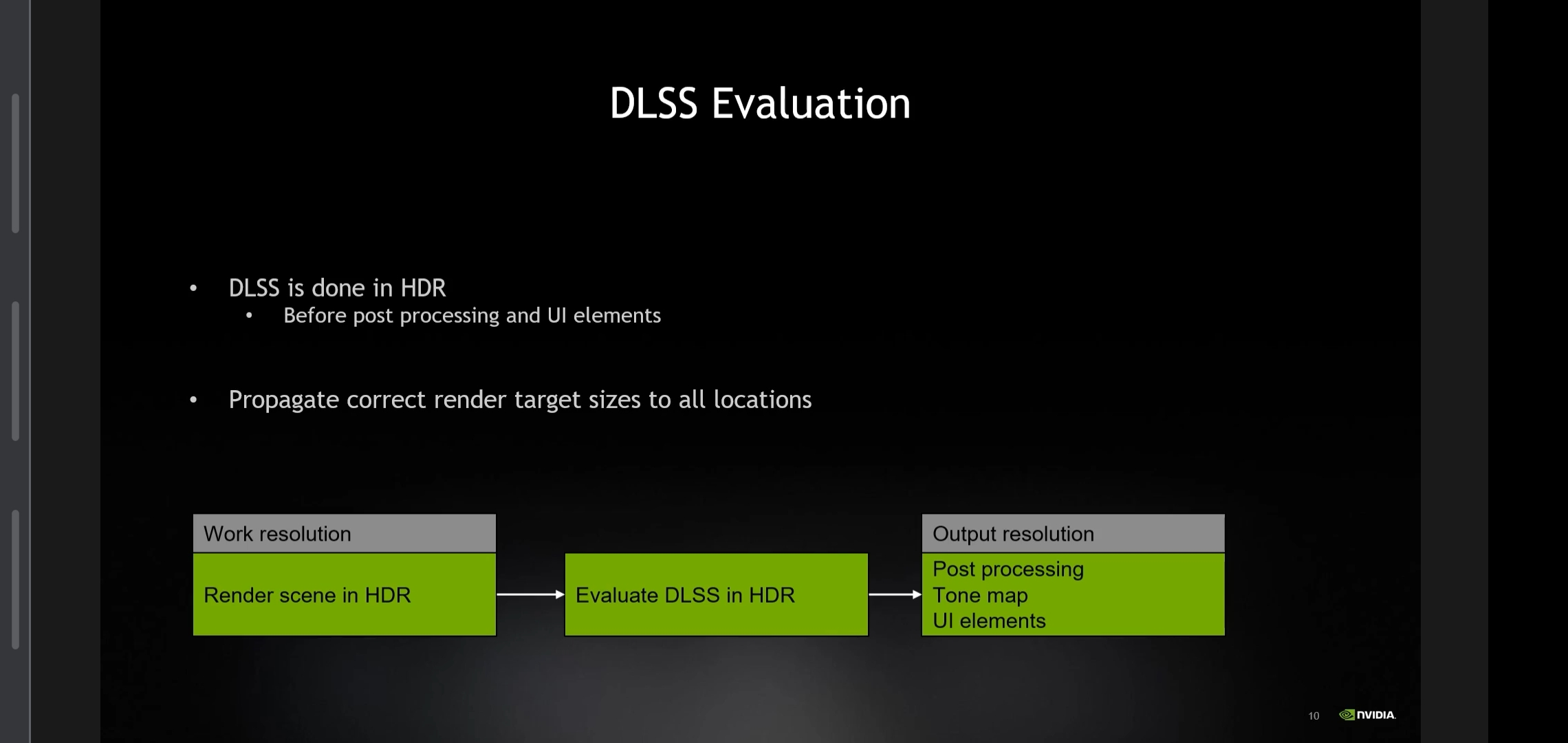
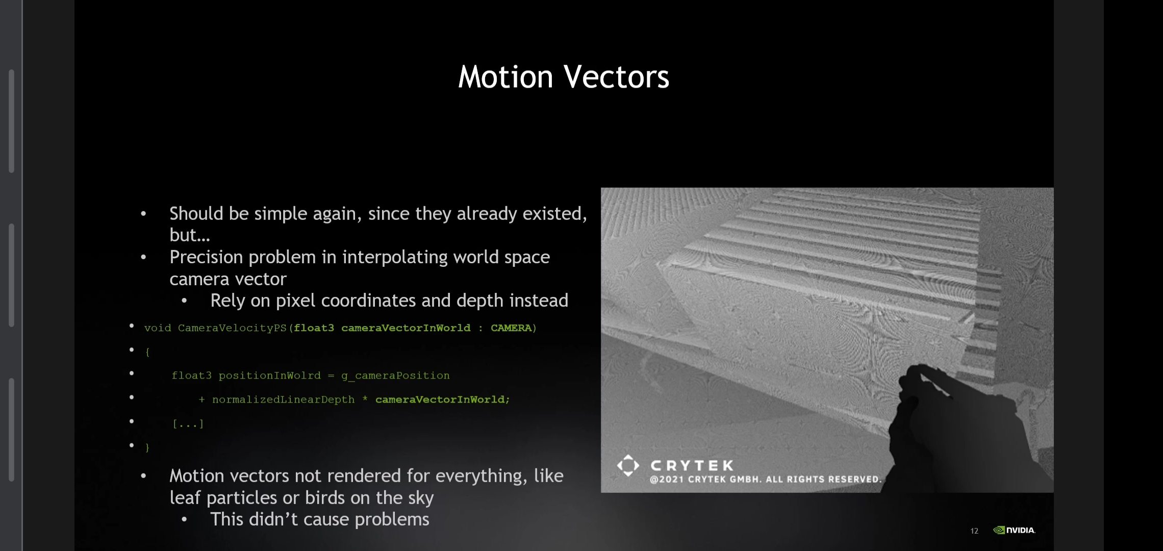
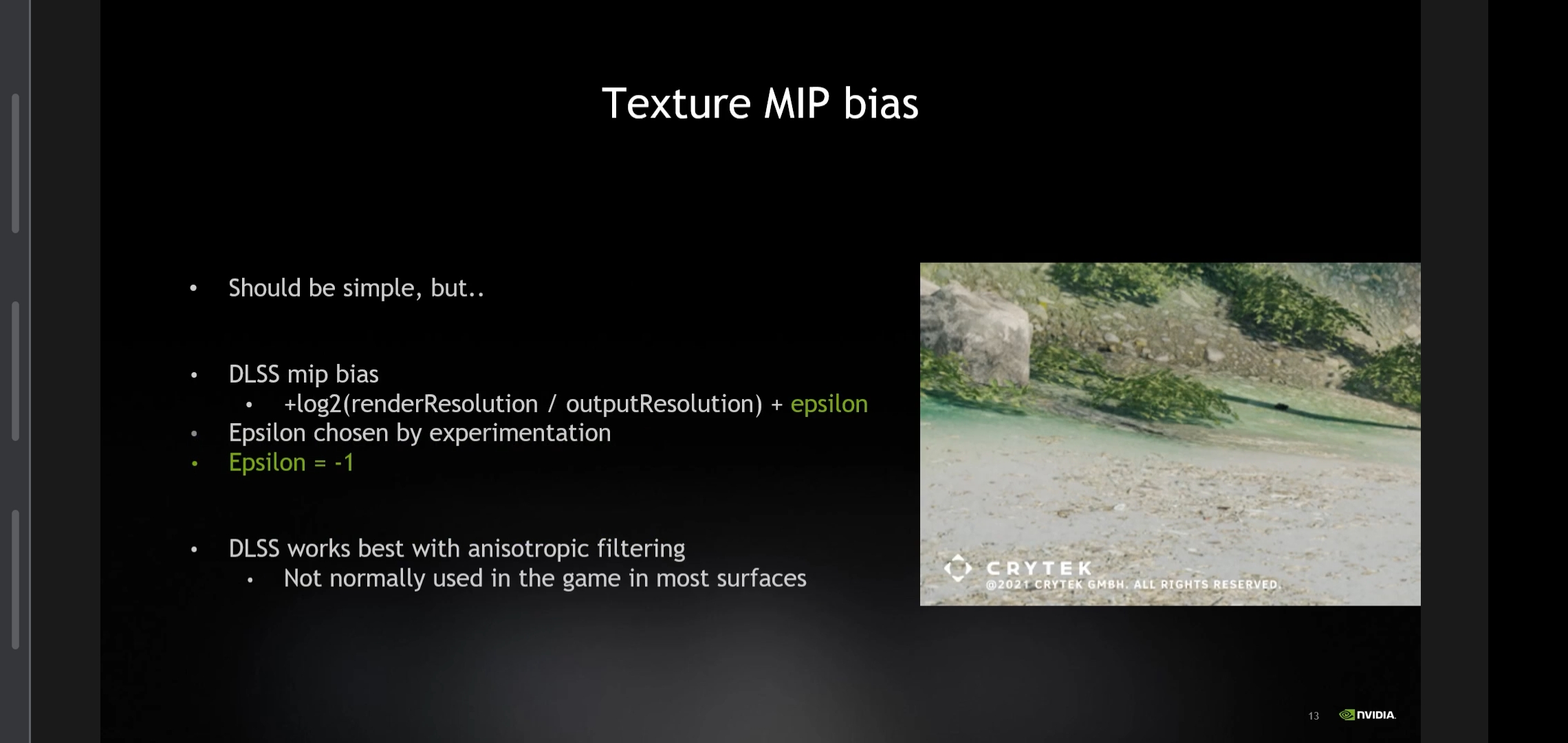
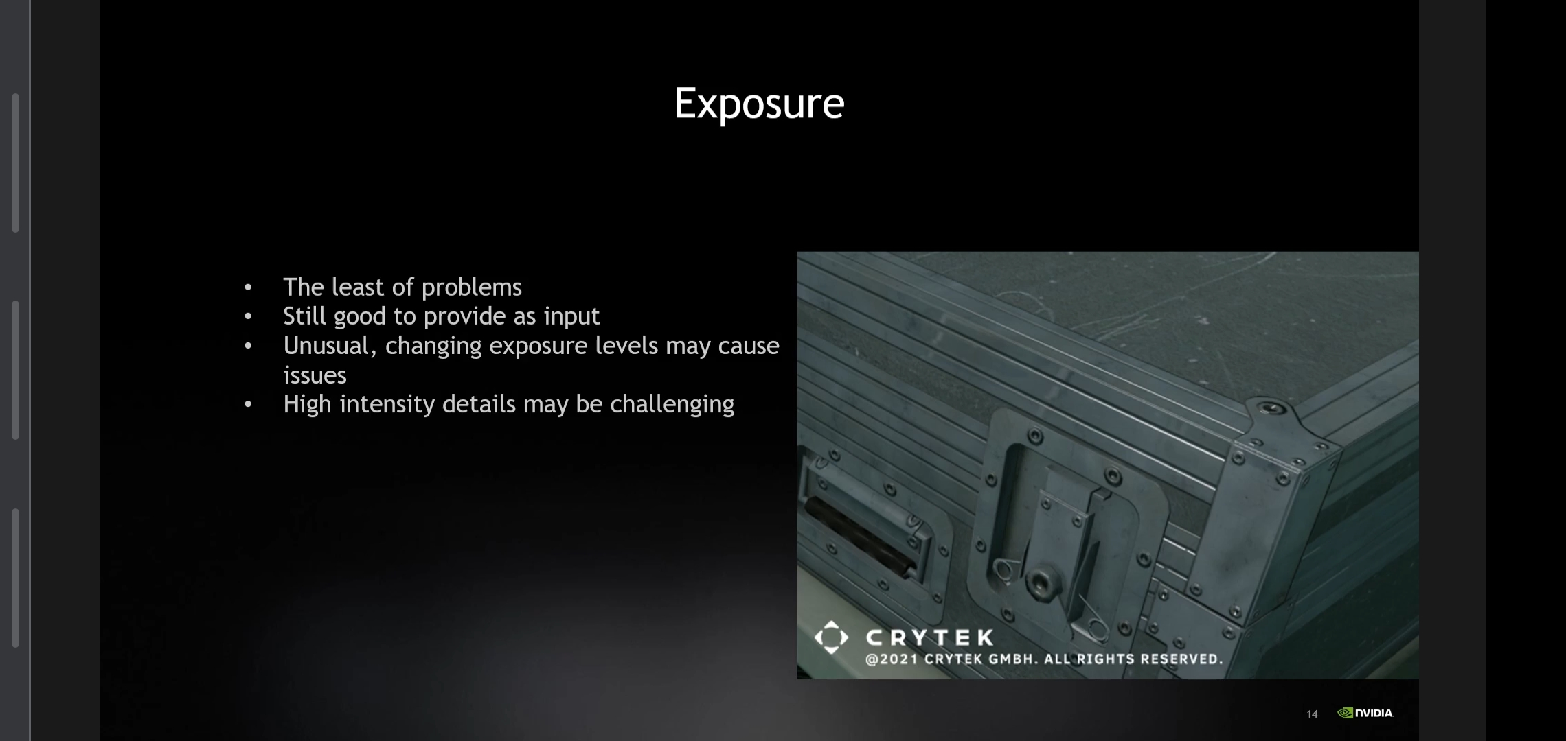
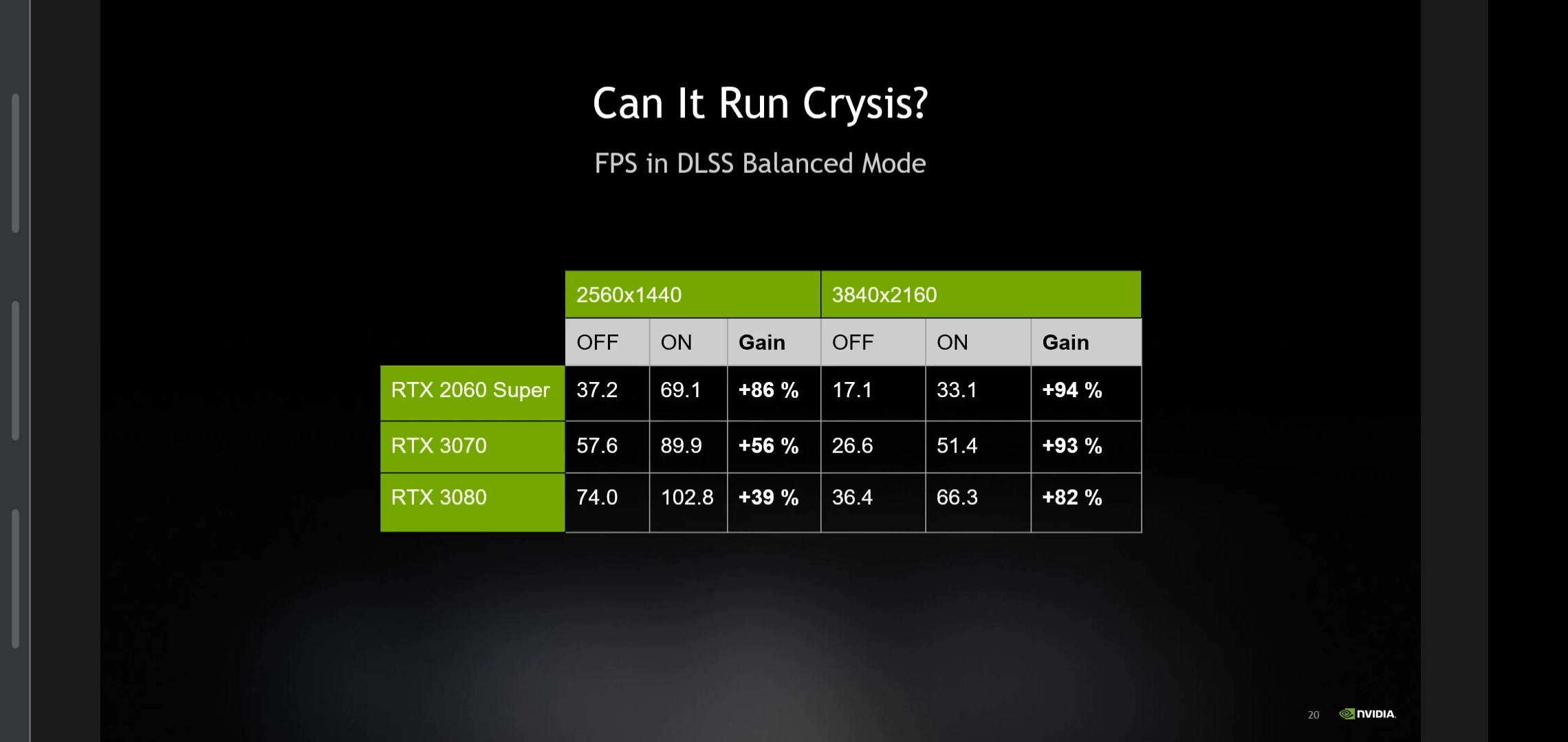
So Crytek shared some tidbits at GTC about integrating DLSS into their engine, which provides some insight on the kind of work that should be expected for 3rd parties adopting the tech for development projects.

Screenshot2021041916.jpg

2faScreenshot2021041916.jpg

6ddScreenshot2021041916.jpg

63bScreenshot2021041916.jpg

304Screenshot2021041916.jpg

1dcScreenshot2021041916.jpg

Screenshot2021041917.jpg


Probably not as straightforward as people were expecting, which is especially important when considering what kind games can be expected to be performant on a DLSS capable Switch. Engine feature compatibility will inevitably play a large role in what DLSS capable games will be developed for or ported to a DLSS capable Switch, so it would be best to set expectations according to how much you see a particular developer willing to invest in making sure that DLSS works well on a DLSS capable Switch. In fact, this applies to any potential DLSS capable console in the future.

So yeah, no magical 'DLSS ON' button for developers, sorry.

I don't have a public link for the talk so if anyone needs clarification on the slides just let me know and I'll do my best to break it down (for the most part the presenter just re-iterated the bullet points you see in the slides).