It all comes down to how much power 8 A78 cores would draw at different frequencies I think. You mention that 12 A78 cores could match Zen 2 at 3 GHz - despite being an unrealistic setup, of course. Well, how about 8 at 1.8 GHz? That would give you core count parity (which I could see make porting code easier than when you have fewer cores) and would give 40% of the CPU performance of a 12 A78 3 GHz rival to the Zen2 8 core setup, which would bring us much closer to next gen performance than the Switch was (which was what, 23% of XB1?). Some current gen ports are possible even with the wide disparity in CPU power between Switch and XB1/PS4 (it was pretty interesting to learn how Saber Interactive modified Witcher 3 to run on the Switch), so closing that gap should progressively make more and more ports possible, even if some of the most demanding games may turn out to be unfeasible still. You've mentioned it's difficult to find power draw for a specific core (because they are usually combined into an actual SoC, which does more than just run the CPU chip), so it's difficult to say what power draw we'd be looking at. But you're probably right that the 1.8W budget for the CPU needs to be expanded a bit in order to be a little bit more competitive. I believe z0m3le did some informed guesstimath on what a possible power profile for such an A78 setup was a while ago, perhaps he can re-iterate that once more.
Quite a while ago I did some calculations across a range of scenarios based on Geekbench 5 FP scores (far from the best comparison, but the only one available for all the CPUs in question), and came up with a best case scenario of a Switch 2 (on 5nm) hitting about 30%-40% of the CPU performance of the PS5/XBSX. (Can't quite find the post right now, this is just off the top of my head) It's impressive given the huge difference in power consumption, and close enough for some ports, but far enough that any large scale systems-based game, say most of Ubisoft's open world games, would have significant difficulty being ported.
Besides, my point wasn't that Nintendo can't build a device which could get some PS5/XBSX ports, or even that they won't. My point was that Nintendo won't design a new Switch with the specific intention to get PS5/XBSX ports. If we're trying to speculate about what hardware Nintendo might release as a Switch "pro" or Switch 2, or whatever, then we should ignore PS5/XBSX, think about what would work best for Nintendo and their partners, and if that ends up being something which can get some next-gen ports then that's a nice bonus.
While I'm not really an experienced practitioner with neural nets, I can provide you with a theoretical answer.
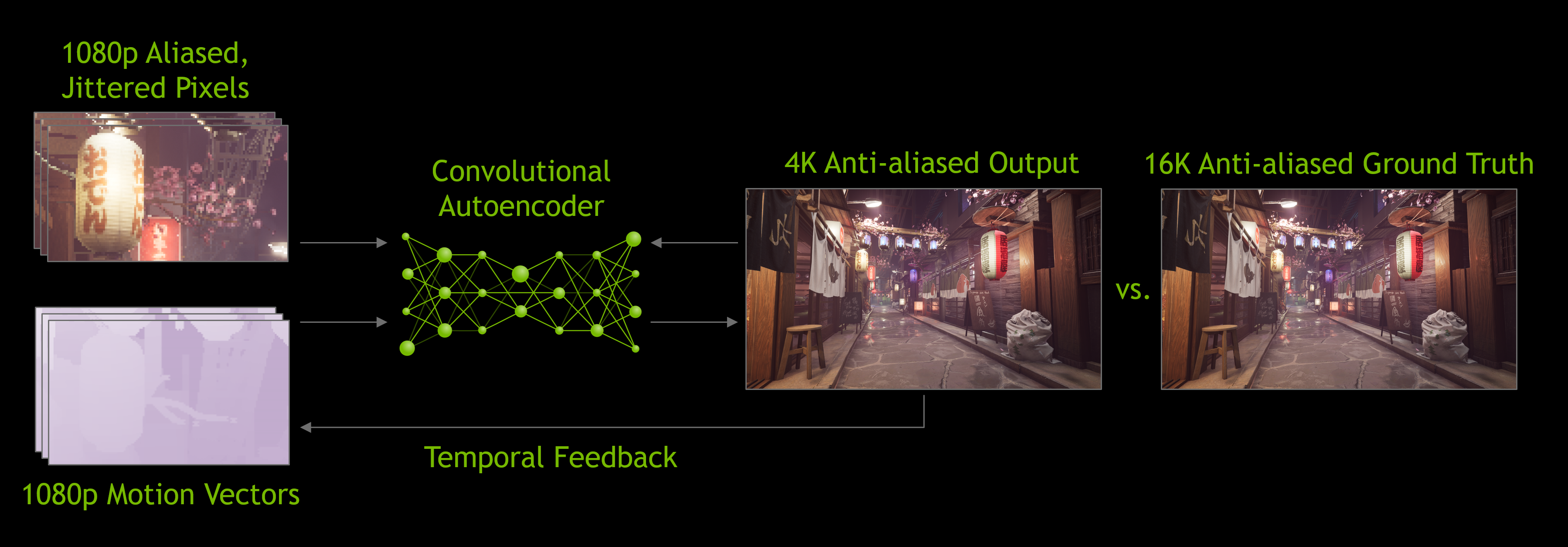
The comparison between image classification and image upscaling is not really apt since the first one is a classification problem but the second one is regression, thus leading to a different (loss/cost) function to optimize. In addition, DLSS does not really add data into the input since it is, at its core, an autoencoder, which by design strives to approximate the input as close as possible in a constrained condition (lossy media encoders are the closest analogs). The reason output images have higher res vs input one is that 1 output image was created using multiple consecutive input images (plus motion vectors, this is why DLSS works very closely with TAA in the rendering pipeline) as shown below:
Besides, my guess for the reason why the DLSS can "add" more details at far distance compared to rendering at native res without DLSS is simply the graphic settings used to generate the ground truth images, e.g tuning up LOD and/or draw distance to maximum. As the result end users will always see the difference since they can never achieve such settings in their machine. Images on their computers must be rendered in real time while ground truth images for training DLSS need not be so.
About pruning, I concur with your assertion that it will reduce accuracy of the algorithm. I think it is a cost NVDIA chose to take in order to have 9x resolution scaling in their next version of DLSS (vs. up to 4x scaling for DLSS 2.0 at the moment) per their Reddit Q&A session. What caught me off guard was, like I stated in my post, the method they used to achieve sparsity for their neural nets: my initial guess was something akin to l1 regularization during training phase then clamp a certain number of weights in the result to 0. But yeah it turned out to be a little bit different: 1st training phase happened normally. Then NVIDIA just straight up cut weights, in a nearly checkerboard pattern, out of the result then compensated the loss by putting the remaining weights through a 2nd training phase.
Edit: after looking at all available info about structural sparsity again, I think my original claim that DLSS 2.0 (and later version) will see increased performance in Ampere may be a little bit premature, since the supposed gain in computation throughput in Ampere's tensor cores clouded my judgement about the performance/quality trade-off for DLSS. The main problem with the claim above is that the current neural net in DLSS 2.0 can be dense. So if NVIDIA wants to utilize Ampere's sparsity leverage on DLSS 2.0, they will have to perform a 2nd training phase for all of their neural nets (for each mode: quality/balanced/perf) as described in the above paragraph, and this can not be verified without benchmarks on current DLSS 2.0-supported games. Unfortunately I have not yet found any RTX 3080 reviews with deep dive into DLSS performance gain in comparison to Turing cards. So in summary:
- It is unknown whether NVIDIA reworked their DLSS 2.0 algorithm to utilize Ampere's structural sparsity, therefore ..
- If NVIDIA want to use Ampere arch on the next Switch and at the same time utilize structural sparsity for DLSS then they will have to refine their current neural nets, as of 2.0 version.
- Whether such refinements on the existing neural nets (for 2x, 3x, and 4x resolution scaling modes) are silently introduced in DLSS 2.0, or will be introduced in later DLSS versions, is an open question. However it is likely that the neural nets for the upcoming 9x scaling mode, expected to come with later DLSS versions, will see this change implemented.
Thanks, that's quite illuminating. It had slipped my mind that multiple frames (including motion vectors) are passed in, hence a lot more input data than I was thinking of.
Regarding the use of L1 regularisation vs a checkerboard-like pattern for the sparsity, my initial thought was that this was down to how the sparsity support is implemented in hardware. Being able to achieve a high speed up with arbitrary sparsity patterns would likely require very complex logic to be implemented in silicon, which would increase size, power draw, and largely defeat the purpose of the tensor cores (which achieve high performance by implementing relatively simple logic on a large scale).
I've done a bit of reading on it, and this diagram is quite instructive (from this post on Nvidia's developer site):

Basically, Ampere's tensor cores operate on 4-element vectors of the weight matrix at once. The sparsity acceleration is achieved by having zero entries for 2 out of the 4 weights in each vector, which allows them to combine two vectors into a single vector for calculation, which gets them their double performance.
So they basically just zero-out the two smallest weights from each 4-element vector and then re-train. Using L1 regularisation wouldn't result in a weight matrix which fits the 2:4 sparsity requirements for Ampere's sparsity acceleration, so simply cutting weights seems like the only way to go about it. I would assume Nvidia have done enough testing to be confident that this can still achieve accurate results. It certainly seems to be a very silicon-efficient way of doing it, in any case.
If Nvidia can apply this sparsity technique to DLSS and achieve good accuracy (theoretically there must be some loss in accuracy, but it may be small enough that a player would not notice), then I would certainly imagine they would re-train their DLSS neural nets to leverage Ampere's sparsity speedup, if they haven't done so already. From the point of view of a hypothetical new Nintendo device, then I'm sure it would be worth re-training, as the cost would certainly be lower than the cost of adding double the tensor cores to the hardware, not to mention increased bandwidth requirements, reduced battery life, etc.
One other interesting point is that it appears the consumer Ampere cards do actually have full-size tensor cores (ie 2x Turing, like A100) on the silicon, but are limited to half that in the GeForce line (so presumably Quadro cards will come out with full-rate support). If this is true, and if DLSS can leverage sparsity acceleration with minimal impact on visual quality, then it changes my expectations on what kind of hardware Nintendo would need to release a DLSS-enabled device in 2021.
I posted a short while ago about what Nintendo might need if they wanted to design a device around using DLSS to achieve 4K output resolution. Based on no sparsity acceleration and the idea that consumer Ampere tensor cores offered the same performance as Turing (without sparsity acceleration), it seemed very unlikely that an affordable portable device could achieve DLSS at 60fps and 4K output resolutions while having to render and perform DLSS sequentially (ie render the frame for approx 75% of the frame time, and spend approx 25% running DLSS). My suggestion was that the shader logic and tensor cores could be decoupled into separate SMs, allowing them to run concurrently (ie run DLSS on one frame while the next is rendering), which would allow 100% utilisation of the tensor cores at the cost of 1 extra frame of latency.
However, assuming sparsity acceleration can be applied to DLSS, and that such a device would get full-rate use of those larger Ampere tensor cores, it actually becomes feasible to achieve DLSS on a standard Ampere tensor core setup within ~4.2ms (1/4 of a frame at 60fps), without the need for customisations to the architecture or additional latency. By my estimates, a 6 SM Ampere GPU at 1.3GHz, or an 8 SM GPU at 1GHz would be able to manage it, which isn't out of the realms of possibility for a Tegra chip designed for a 2021 Switch (for comparison, Xavier uses an 8 SM GPU).
One limitation which might still be there (actually increased, due to the shorter time DLSS has to operate over) would be memory bandwidth. Assuming RTX 2060 is fully bandwidth-limited while running DLSS at 4K (it's probably not, but worst-case scenario), even with a 2x reduction in bandwidth from sparsity, an Ampere GPU would need just over 100GB/s to run it within ~4.2ms. RTX 2060 probably isn't bandwidth-limited, but you're still probably looking at a 128-bit LPDDR4X RAM setup (about 68GB/s) as a realistic requirement.
In fact, I would have ruled out LPDDR5 not that long ago, both based on cost, but also the fact that it was only available in large capacities, meaning a 2x8GB setup would be the only option if they wanted a 128-bit bus, which is well past what I'd expect in a 2021 device. I just had a quick look on it, though, and it looks like Micron are currently sampling a variety of LPDDR5 parts with smaller capacity. What this tells me is that (a) it's actually possible for Nintendo to go as low as 8GB total memory on a 128-bit LPDDR5 bus, but also (b) that there's likely to be a migration of the mid and low end of the smartphone market to LPDDR5 over the next year or so. In particular, they've got a 2GB part with a 32-bit interface, which only really makes sense for the lower end of the market. Nintendo haven't really hesitated on using expensive RAM in the past (they used LPDDR4X on the 2019 Switch and Switch Lite purely for the improved power efficiency), so I wouldn't rule out LPDDR5 either. Two of the 4GB x64 LPDDR5 chips Micron are sampling would give 8GB of RAM and 102.4GB/s of bandwidth, which would be a huge boost over the original Switch. Of course they could go with a single 6GB/8GB module for 51.2GB/s, but I'd be somewhat concerned at DLSS becoming bandwidth-limited at that point.
A hypothetical DLSS-enhanced Switch model in 2021 could actually look pretty nice:
7nm manufacturing process (much like TX1 vs desktop Maxwell, I think there's a benefit to going with a smaller node for power efficiency)
4x A78 @1.6GHz (lets say) for games, with some A55 cores for OS/sleep mode
6x Ampere SMs @1.3GHz docked (maybe ~500MHz portable?)
8GB LPDDR5 on a 128-bit bus for 102.4GB/s
Aside from obviously the DLSS, it's quite a good upgrade from the original Switch, with a substantial CPU boost, probably 2-3x the GPU performance pre-DLSS, and obviously the RAM capacity and bandwidth upgrade.
On top of that, it actually makes sense as a SoC Nvidia might want to position for edge AI applications. Assuming sparsity support and ~1.5GHz peak GPU clock, it would hit 74 TOPS INT8, which is about 2.5x Xavier (without having to mess with it being split between tensor cores and a DLA). It should also be a lot smaller and more power-efficient than Xavier, and potentially cheaper than Xavier given the smaller CPU/GPU configurations. It would also support up to 32GB of RAM, or more as larger LPDDR5 modules come along.
That's not to say I'd expect such a chip, but it's not entirely outside the realms of possibility for a reasonably-priced Nintendo device in 2021, and it's interesting to consider.