What do you think could be the memory setup of your preferred console, or one of the new consoles?

  • GDDR6

    Votes: 566 41.0%
  • GDDR6 + DDR4

    Votes: 540 39.2%
  • HBM2

    Votes: 53 3.8%
  • HBM2 + DDR4

    Votes: 220 16.0%

  • Total voters
    1,379
Status
Not open for further replies.

Pheonix

Banned
Dec 14, 2018
5,990
St Kitts
Could this be the basis of the 2 console strategy from MS though? What if you take those chips for the lower end console, wouldn't that work out?
Technically yes. But even that was shot down a while ago. Think that's more to do with how different the two skus were If one was 10Tf and the other was 8TF then that could be achieved using the same chip. But if one is 10TF and the other is 4-6TF ten its silly using the same chip cause that's a waste of chip lol.

However, the need for two SKUs is even more unlikely when if (as it appears to be) sony is spending as much for their base and only console as what MS was going to spend for their premium console. Means there is no premium console anymore and now getting the most bang for your buck as reasonably as possible take precedence.
 

Liabe Brave

Professionally Enhanced
Member
Oct 27, 2017
1,672
I know you, anex and duke dont want to put too much faith in it but your die size calculations has given team 12.9 tflops new life. If the die size is indeed 400+, 54-56 CU is on the cards.
The die size is uncertain and could actually be less than 400mm^2; it could also be over, but in neither case is the variance by very much. And even the largest chip would be very hard to fit 56 active CUs. Remember that you have to physically include at least 4 extra, so by disabling some you can absorb mildly defective products. So here's the math: Zen 2 would be ~70mm^2. Navi 10 is 251mm^2. Adding another SE would be ~73mm^2 (to get 56 active CUs, ). Another memory controller would add ~13mm^2.

That's already 410mm^2, and it doesn't include any space for the RT hardware that we know the console has. In other words, it's very unlikely Anaconda will contain 56 active CUs. The ceiling is probably 52 (active). And the final number will likely be lower still; I think the prevalence of high guesses is based in "Navi is GCN" calculations of how much room the 7nm node would provide. I myself was also previously bullish on this, but now we know that RDNA CUs are quite a bit evolved and require more transistors than their GCN predecessors. So not as many will fit anymore, and I think people haven't really absorbed that yet.

If Sony was planning their hardware and already had people developing with an initial release of let's say holidays 2019, how could they have something more powerful than someone planning for 1 year later...?
The suggested scenario is because they changed to a 2020 target a while ago, not this year. Companies often lay the groundwork for an array of possibilities, and then only drive one version to completion. But this means there's an opportunity to halt and switch to another plan, a later and stronger device. For example, Phil Spencer said that Microsoft considered a machine around the power level of PS4 Pro to release in 2016, but decided against it and went with the later, more powerful One X plan instead.

Could this be the basis of the 2 console strategy from MS though? What if you take those chips for the lower end console, wouldn't that work out?
That only really makes sense if the two offerings are relatively close to each other. If the low-end machine is only half the power of the premium one--and all rumors say Lockhart is that level or even lower compared to Anaconda--then it's no longer logical. You get to salvage the chips too defective for Anaconda, sure...but they're twice as big as you need for Lockhart, so you end up paying a lot more per piece for the most expensive component of your "cheap" console.

One thing to keep in mind is that the two-SKU approach is a way to mitigate costs and reduce risk, not an indicator of greater willingness to absorb losses. (Even though lots of folks interpret it backwards this way.)
 

Hey Please

Avenger
Oct 31, 2017
22,824
Not America
After having seen the latest RDNA pdf that posted here, I was hoping whether someone can clarify if 5700 series gone back to 2 Shader Engines per "Dual" or 20 CUs and whether this has significant ramifications for next gen systems.
 

Deleted member 12635

User requested account closure
Banned
Oct 27, 2017
6,198
Germany
After having seen the latest RDNA pdf that posted here, I was hoping whether someone can clarify if 5700 series gone back to 2 Shader Engines per "Dual" or 20 CUs and whether this has significant ramifications for next gen systems.
I would think they just cut/deactivated one WGP per Shader Engine which makes 4 CUs in total with a remaining 36CUs.

Btw, what PDF?
 

Pheonix

Banned
Dec 14, 2018
5,990
St Kitts
After having seen the latest RDNA pdf that posted here, I was hoping whether someone can clarify if 5700 series gone back to 2 Shader Engines per "Dual" or 20 CUs and whether this has significant ramifications for next gen systems.
I have been here trying to hammer the same thing down to. But from my understanding of things (having looked at the chip images) and from what have said.... I am inclined to stick with my original conclusion that there are now two shader engines.

So then it used to be GCU> SE> CU. Now its GCU> SE> WG > CU.

Basically, the workgroup (WG) consist of a pair of CUs. And from what I gather, the reliance on the shader engine 'gateway" is a lot less now. More granular control to the WGs.
 

Hey Please

Avenger
Oct 31, 2017
22,824
Not America
I would think they just cut/deactivated one WGP per Shader Engine which makes 4 CUs in total with a remaining 36CUs.

Btw, what PDF?

Thanks.

Also, the pdf:

https://gpureport.cz/info/Graphics_Architecture_06102019.pdf

If you have not seen this, it may be prove far more useful to you.

I have been here trying to hammer the same thing down to. But from my understanding of things (having looked at the chip images) and from what have said.... I am inclined to stick with my original conclusion that there are now two shader engines.

So then it used to be GCU> SE> CU. Now its GCU> SE> WG > CU.

Basically, the workgroup (WG) consist of a pair of CUs. And from what I gather, the reliance on the shader engine 'gateway" is a lot less now. More granular control to the WGs.

Guess it is wait and watch until it is made absolutely affirmative in the release version break downs by third parties. Thank you.
 

anexanhume

Member
Oct 25, 2017
12,939
Maryland
I have been here trying to hammer the same thing down to. But from my understanding of things (having looked at the chip images) and from what have said.... I am inclined to stick with my original conclusion that there are now two shader engines.

So then it used to be GCU> SE> CU. Now its GCU> SE> WG > CU.

Basically, the workgroup (WG) consist of a pair of CUs. And from what I gather, the reliance on the shader engine 'gateway" is a lot less now. More granular control to the WGs.
You mean scalable? ;)
 

Pheonix

Banned
Dec 14, 2018
5,990
St Kitts
You mean scalable? ;)
lol... I would be lying i told you that's what I meant. But I will apt that as the proper term to describe what I was trying to say lol.
10GB HBM and 16GB DDR4 with 4GB of DDR4 reserved for the OS. 22GB of RAM that appears as one pool for devs.

🙏🏾
It's bad enough you are already praying for the unlikely then you go and make the prayer even more unlikely by putting 10GB HBM??

If HBM2 doesn't happen I'm blaming you, we have to keep our prayers focused as not to confuse the man upstairs.
 

AudiophileRS

Member
Apr 14, 2018
378
I was very much in the 12-14TF camp before but given recent developments I'm both expecting and would be very happy with 10-11TF. 48-54CU @ 1450-1650Mhz seems like the sweet spot to me.

I wouldn't be surprised by a peak 200w console, a 400mm2 APU die and a $499 retail.

My only real concern right now is RAM,.. but aside from that I'm beginning to feel very positive about the next-gen, technically speaking.

------------------------

Regarding memory and riffing off 'that rumour'; I'd love to see something like this as a nice middle ground in PS5:

MEMORY SYSTEM
  • HBM2/3 | 12GB @ ~537GB/s | On-SoC Fan-Out Design + Underside Heatsink (2 Stacks x 6-Hi x 8Gb @ 1050MHz, 2048-Bit Bus)
  • DDR4 | 12GB @ ~70GB/s | Off-SoC 3 Per-Side (6 x 16Gb 32-Bit I/O @ 2933MHz, 192-Bit Bus)
  • Embedded Hi-Endurance SSD Scratchpad w/ SRAM Cache | >100GB @ ~5GB/s Read, ~3GB/s Write, PCIe 4.0 On-SoC Storage Controller
  • HBCC & Optimised I/O Stack
  • HBM & DDR appear as single unified memory pool by default with multiple layers of abstraction available for further optimisation.
 

Lagspike_exe

Banned
Dec 15, 2017
1,974
Maybe but I still would have expected to hear something by now. Either a leak within the gaming or tech sites or on the component or manufacturing side.

To be perfectly honest, that part of the leak sounds perfectly rationa. Considering PS4 tail sales and that it will most likely sell probably over 20m units after PS5 introduction, it makes no sense to keep it on 16nm process. Cell and RSX were die shrinked to 45nm (I think RSX even got a 28nm shrink). Shrinking just one chip is even cheaper.
 

anexanhume

Member
Oct 25, 2017
12,939
Maryland
To be perfectly honest, that part of the leak sounds perfectly rationa. Considering PS4 tail sales and that it will most likely sell probably over 20m units after PS5 introduction, it makes no sense to keep it on 16nm process. Cell and RSX were die shrinked to 45nm (I think RSX even got a 28nm shrink). Shrinking just one chip is even cheaper.
Cell was supposedly shrunk to 22nm.


Xeontech

Member
Oct 28, 2017
4,059
To be clear, I am firmly in the 56cu 1.8Ghz camp. 12tf+ all the way.

It's custom, and coming at the end of 2020. Absolutely conceivable regardless what we heard announced this week.

I am also firmly in the HBM camp for at least one of the next gen consoles.
 
Jul 6, 2018
174
A flop is a number of performance at always 100% utilization of all stream processors at all time (peak performance). That is a theoretical number that will never happen. However the thing you want achieve is to get your real performance as near as possible to that theoretical number. This is what I call "efficiency" (how efficient do I make use of the hardware resources and reduce forced idle times because of bottlenecks). Perf per Clock is a delta value and a way how you can compare architectures on their efficiency.
You do not seem to understand what I am saying. I am not saying that clocks and flops are the same thing. What AMD refers to as performance per clock is directly proportional to performance per flop when comparing RDNA and GCN cards. Therefore, comparing the performance per flop or per clock of one RDNA or GCN GPU to another as a ratio will produce an identical result.
 

Locuza

Member
Mar 6, 2018
380
After having seen the latest RDNA pdf that posted here, I was hoping whether someone can clarify if 5700 series gone back to 2 Shader Engines per "Dual" or 20 CUs and whether this has significant ramifications for next gen systems.
Previously AMD called a Shader Engine a whole slice of the GPU.
gcn-architektur-2.png


There was one Geometry Processor and Rasterizer, then the Shader Array consisting of a certain number of CUs (up to 16 under GCN) and the Rendering Backends (Up to 4 Render Backends/16 ROPs).
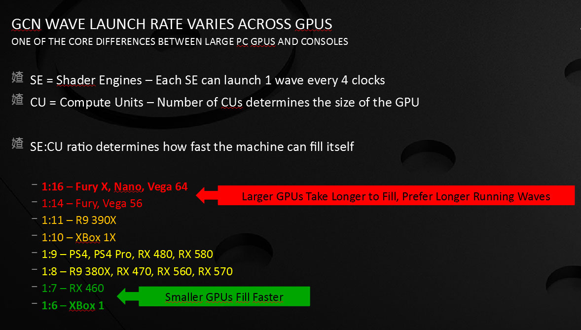
One Issue about the Shader Engine design for GCN was that with more CUs it was harder for the Shader Engine to feed them all if the workload was too short and the CUs would compute it faster than the SE could feed them.
amdrate7nuxr.jpg


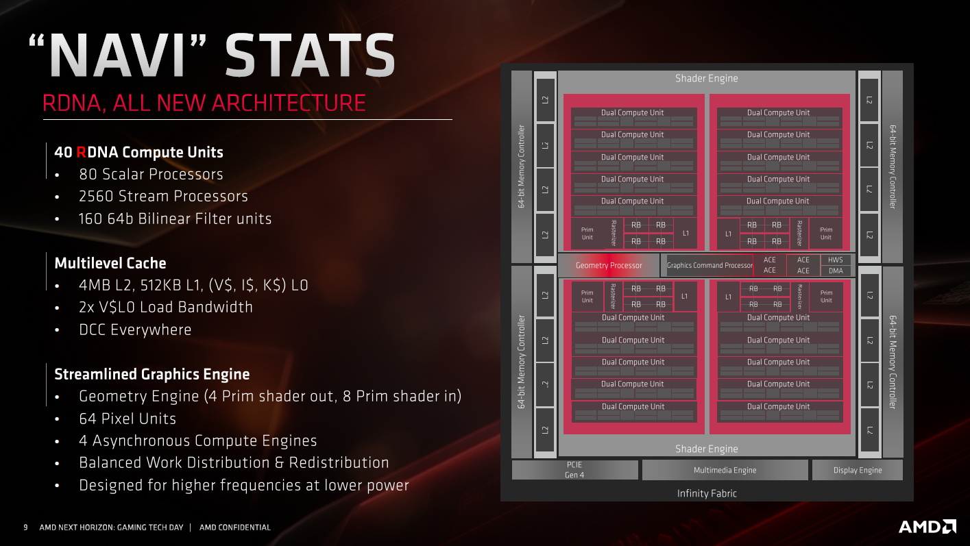
The diagram for Navi10 shows actually no logical connection as to why it would be two Shader Engines.
In comparison to earlier it would be 4 Shader Engines (the blocks in red).
17-1080.a19d7014.jpg


Under Navi 10 one slice seems to be 1 Prim Unit, 1 Rasterizer, a certain number of CUs (5 WGPs/10 CUs under Navi10), 4 Render Backends (16 ROPs) and 128KB of L1$ (at least for Navi10).
The Wave Launch Rate wasn't specified but AMD probably made sure that this wouldn't be an issue.
 
Last edited:

disco_potato

Member
Nov 16, 2017
3,145
To be clear, I am firmly in the 56cu 1.8Ghz camp. 12tf+ all the way.

It's custom, and coming at the end of 2020. Absolutely conceivable regardless what we heard announced this week.

I am also firmly in the HBM camp for at least one of the next gen consoles.

From my understanding X had a very early 580 on a larger node that the 580 itself. PRO has a sub rx 470 equivalent. Xbone and ps4 launched with a gpu from early 2012. Last 4 consoles launched with GPUs based in desktop parts released in years prior to their release or ones from the value segment. Is it reasonable to expect 2020 GPUs in 2020 consoles? Or is it more likely we'll get 2019 GPUs with some tech taken from 2020 GPUs?
 
Jul 6, 2018
174
From my understanding X had a very early 580 on a larger node that the 580 itself. PRO has a sub rx 470 equivalent. Xbone and ps4 launched with a gpu from early 2012. Last 4 consoles launched with GPUs based in desktop parts released in years prior to their release or ones from the value segment. Is it reasonable to expect 2020 GPUs in 2020 consoles? Or is it more likely we'll get 2019 GPUs with some tech taken from 2020 GPUs?

That's not really the correct way of looking at it. It's more like AMD puts out cards based on the parts it's working on for its semi-custom customers than the other way around. PS4 and Xbox One GPUs (Liverpool and Durango) are 2nd Gen GCN. The first 2nd Gen part wasn't released till March 2013, 8 months before the consoles launched. It had fewer CUs than the PS4, but a faster clock.
 

Locuza

Member
Mar 6, 2018
380
From my understanding X had a very early 580 on a larger node that the 580 itself. PRO has a sub rx 470 equivalent. Xbone and ps4 launched with a gpu from early 2012. Last 4 consoles launched with GPUs based in desktop parts released in years prior to their release or ones from the value segment. Is it reasonable to expect 2020 GPUs in 2020 consoles? Or is it more likely we'll get 2019 GPUs with some tech taken from 2020 GPUs?
Both Xbox One and PS4 actually used GCN Gen 2, which came early 2013 to the Desktop in form of the Bonaire chip (7790) from AMD.

The PS4 Pro had major Polaris features (Primitive Discard Accelerator, Delta Color Compression) and two features which only later came to the PC with Vega (at the end of Q2 2017) which were RPM (Rapid Packed Math /2xFP16) and the IWD (Intelligent Workload Distributor).

The Xbox One X seems to only use the Polaris tech.

But all console designs are unique and had no 1:1 part on the PC side.

To the question in the end, it could be anything.
It depends on the development window of AMDs own tech and what timelimes Sony and MS gave to AMD and what custom work was done.
It could be RDNA 1 + some stuff from RDNA 2, it could be RDNA1 + more stuff of RDNA 2 or it could be RDNA1 with rather unique custom work with Sony and MS where AMD won't be using the exact same implementation for RDNA2.
In the best case it is RDNA2.
 

AegonSnake

Banned
Oct 25, 2017
9,566
Anyone who thinks either next gen will be more then 11tflops is going to lose.
thats what they said about the SSD.

thats what they said about Ray tracing.

Thats what they said about PS5 not going above $399.

Just last week we all believed the reddit rumor that the die was goingto br 311 mm2 and now the Scarlett die is definitely over 350mm2 and maybe even 400 mm2 and it still has Phil wondering if thats enough.

We in uncharted territory now.
 

Lagspike_exe

Banned
Dec 15, 2017
1,974
I wouldn't be surprised considering they have to use it in PSNow and they were probably aware that even next gen hardware won't be able to emulate it or even if it could, it would require enormous processing power.
People on the message boards have been generally underestimating PlayStation hardware team and calling PS4 just a random stroke of luck, but they've made a lot of intelligent decisions over time that have added up to produce great results. I have a lot of fate in them regarding PS5.
 

Pheonix

Banned
Dec 14, 2018
5,990
St Kitts
Previously AMD called a Shader Engine a whole slice of the GPU.
gcn-architektur-2.png


There was one Geometry Processor and Rasterizer, then the Shader Array consisting of a certain number of CUs (up to 16 under GCN) and the Rendering Backends (Up to 4 Render Backends/16 ROPs).
One Issue about the Shader Engine design for GCN was that with more CUs it was harder for the Shader Engine to feed them all if the workload was too short and the CUs would compute it faster than the SE could feed them.
amdrate7nuxr.jpg


The diagram for Navi10 shows actually no logical connection as to why it would be two Shader Engines.
In comparison to earlier it would be 4 Shader Engines (the blocks in red).
17-1080.a19d7014.jpg


Under Navi 10 one slice seems to be 1 Prim Unit, 1 Rasterizer, a certain number of CUs (5 WGPs/10 CUs under Navi10), 4 Render Backends (16 ROPs) and 128KB of L1$ (at least for Navi10).
The Wave Launch Rate wasn't specified but AMD probably made sure that this wouldn't be an issue.
I doubt there are 4 SE like before.

First of that would mean that if disabling CUs you would have to disable one workgroup in each SE. Resulting in the loss of 8 CUs.

Then there this is the 36CU RX5700. That is no doubt a descendant of the RX5700XT. And only 4 CUs (two workgroups, one in each SE) were disabled.

Unless you are suggesting that in each WG, they can choose to disable only one of the paired CUs.
 

disco_potato

Member
Nov 16, 2017
3,145
That's not really the correct way of looking at it. It's more like AMD puts out cards based on the parts it's working on for its semi-custom customers than the other way around. PS4 and Xbox One GPUs (Liverpool and Durango) are 2nd Gen GCN. The first 2nd Gen part wasn't released till March 2013, 8 months before the consoles launched. It had fewer CUs than the PS4, but a faster clock.
Both Xbox One and PS4 actually used GCN Gen 2, which came early 2013 to the Desktop in form of the Bonaire chip (7790) from AMD.

The PS4 Pro had major Polaris features (Primitive Discard Accelerator, Delta Color Compression) and two features which only later came to the PC with Vega (at the end of Q2 2017) which were RPM (Rapid Packed Math /2xFP16) and the IWD (Intelligent Workload Distributor).

The Xbox One X seems to only use the Polaris tech.

But all console designs are unique and had no 1:1 part on the PC side.

To the question in the end, it could be anything.
It depends on the development window of AMDs own tech and what timelimes Sony and MS gave to AMD and what custom work was done.
It could be RDNA 1 + some stuff from RDNA 2, it could be RDNA1 + more stuff of RDNA 2 or it could be RDNA1 with rather unique custom work with Sony and MS where AMD won't be using the exact same implementation for RDNA2.
In the best case it is RDNA2.

Thanks for clearing that up. TPU shows xbone as gcn 1 though. Guessing that's incorrect?
 

Rylen

Member
Feb 5, 2019
475
To be clear, I am firmly in the 56cu 1.8Ghz camp. 12tf+ all the way.

It's custom, and coming at the end of 2020. Absolutely conceivable regardless what we heard announced this week.

I am also firmly in the HBM camp for at least one of the next gen consoles.

I'm team 56 CU as well.

But between 1650-1700 MHz
 

AegonSnake

Banned
Oct 25, 2017
9,566
Navi 10 is 251mm^2. Adding another SE would be ~73mm^2 (to get 56 active CUs, ). Another memory controller would add ~13mm^2.

but if it's already over 350mm2 and under 400 mm2, the gpu alone is already larger than the 251mm2 Navi 5700XT chip even after the 70mm2 zen2 cpu. to me that means MS already has that third SE in their roughly 350-400mm2 GPU with all the memory controllers and RT hardware they need.

I am assuming 1 SE is 20 CUs, and the two Navi chips releasing this year are 2 SEs. So i guess MS already has 3 SEs with 60 CUs at 400mm2 or 390 mm2 or whatever you guys calculated. 4 disabled (or do they now need to disable 6?) to get 54-56 CUs. Lower Clocks than the 5700 XT at around 1.5ghz for 11 tflops. If i was Phill, i would be pretty bullish.

but then Sony sees MS go for 350+mm2 chip and thinks to themselves, why stick with 350mm2 like we did for our $399 PS4 when we have an extra $100 to play with. why pay $100 for an APU like we did for the PS4 when we can pay $150 for an APU with an extra $20 in vapor chamber or other fancy form for cooling and still have $30 to play with?

400 mm2 would still be less than size of the cell and the rsx. more powerful and not nearly as expensive.

Where is the die size rumor coming from? 400 would be massive
From here. Dukeblueballs estimated the Scarlett chip to be around 390mm2. Anex and pheonix also agreed that its around 400mm2 in size, maybe even bigger but they arent sure. Richard Ledbetter couldnt tell from the SoC what the size was but i dont think he looked as hard as these guys.
Alright broke out the measurement taping and found out some things about Navi and the Anaconda in terms of sizes on 7nm.
RX 5700 XT die:
GDDR6 phy controller: 4.5mm x 8
Dual CUs: 3.37mm x 20
4 ROP cluster: .55mm x 16
L1+L2+ACE+Gemotry processor+empty buffer spaces + etc: 139mm

Now Anaconda:

A rougher estimate using the 12x14mm GDDR6 chips next to the SOC.

380mm-400mm.

It's a bit bigger than the 1X SOC for sure.

If we use the figure of 390mm,

70mm for CPU
45mm for 10 GDDR6 controllers
8.8mm for ROPs
150mm for buses, caches, ACE, geometry processors, shape etc. I might be over estimating this part as the 5700 seems to have lots of "empty" areas.

We have ~115mm left for CUs + RT hardware. There is enough there for ~32 dual CUs and RT extensions.

Conclusion:

The Anaconda SOC is around the minimum size you need to fit the maximum (64 CU) Navi GPU and Zen2 cores.
I expect Anaconda to have a minimum of 48 active CUs if the secret sauce is extra heavy or maximum active 60CUs if the sauce is light.
 
Last edited:

Locuza

Member
Mar 6, 2018
380
I doubt there are 4 SE like before.

First of that would mean that if disabling CUs you would have to disable one workgroup in each SE. Resulting in the loss of 8 CUs.

Then there this is the 36CU RX5700. That is no doubt a descendant of the RX5700XT. And only 4 CUs (two workgroups, one in each SE) were disabled.

Unless you are suggesting that in each WG, they can choose to disable only one of the paired CUs.
That's what I assume when AMD wants the load balancing to be evenly between the shader arrays.

Otherwise I see currently no logical point or difference between two or four Shader Engines.

Let's say you have two Shader Engines but each SE has two blocks where each one has 1 Prim Unit, 1 Rasterizer, up to 5 WGPs, 4 RBs and 128KB L1$.

If you deactivate one WGP then one half of the Shader Engine is unlike the other and I don't see the argument against four Shader Engines having the same imbalance.
There is no Scheduler/Fetch/Dispatch-Unit of sorts in the diagram so from that view I see no high level unit consisting of two Shader Engines.

Thanks for clearing that up. TPU shows xbone as gcn 1 though. Guessing that's incorrect?
Yes, that's not right.
It has two ACEs with 16 compute queues in total while GCN1 always had two ACEs with just 2 compute queues in total.
Another aspect is the unified memory where GCN1 was lacking system unified adressing.

From a Digitial Foundry Interview:
Andrew Goossen first confirms that both Xbox One and PS4 graphics tech is derived from the same AMD "Island" family before addressing the Microsoft console's apparent GPU deficiency in depth.

Just like our friends we're based on the Sea Islands family (...)
https://www.eurogamer.net/articles/digitalfoundry-vs-the-xbox-one-architects

Sea Islands = GCN Gen 2:
http://developer.amd.com/wordpress/media/2013/07/AMD_Sea_Islands_Instruction_Set_Architecture.pdf

There was the technical marketing fuck up from AMD where they also used Sea Islands as an umbrella for the whole product family in 2013 which led to quite some confusion.
 

Rylen

Member
Feb 5, 2019
475
From my understanding X had a very early 580 on a larger node that the 580 itself. PRO has a sub rx 470 equivalent. Xbone and ps4 launched with a gpu from early 2012. Last 4 consoles launched with GPUs based in desktop parts released in years prior to their release or ones from the value segment. Is it reasonable to expect 2020 GPUs in 2020 consoles? Or is it more likely we'll get

2019 GPUs with some tech taken from 2020 GPUs?

Except there's only 1 measly GPU this time around.

With PS4 there were many GCN cards to speculate from, and we ended up getting what I would call the "8"series GCN...HD Seventy8Fifty

Right now AMD has only shown the "7" series RDNA, RX Fifty7Hundred XT perhaps by request from Sony/MS not to show their hand regarding next consoles
 

Rylen

Member
Feb 5, 2019
475
but if it's already over 350mm2 and under 400 mm2, the gpu alone is already larger than the 251mm2 Navi 5700XT chip even after the 70mm2 zen2 cpu. to me that means MS already has that third SE in their roughly 350-400mm2 GPU with all the memory controllers and RT hardware they need.

I am assuming 1 SE is 20 CUs, and the two Navi chips releasing this year are 2 SEs. So i guess MS already has 3 SEs with 60 CUs at 400mm2 or 390 mm2 or whatever you guys calculated. 4 disabled (or do they now need to disable 6?) to get 54-56 CUs. Lower Clocks than the 5700 XT at around 1.5ghz for 11 tflops. If i was Phill, i would be pretty bullish.

but then Sony sees MS go for 350+mm2 chip and thinks to themselves, why stick with 350mm2 like we did for our $399 PS4 when we have an extra $100 to play with. why pay $100 for an APU like we did for the PS4 when we can pay $150 for an APU with an extra $20 in vapor chamber or other fancy form for cooling and still have $30 to play with?

400 mm2 would still be less than size of the cell and the rsx. more powerful and not nearly as expensive.

1.5 GHz seems unnecessarily underclocked.

When GCN1 released the 7870 GHz Edition was 20 CU, 1000mhz, and 175w

8 months later 7870 XT released with 24 CU, 975mhz, and 185w

That's 20% more CU
2.5% less clocks
6% more Power Draw
18% more Teraflops

Seems like you can add lots of CU, and lower clocks very very little and get the same power draw from the GPU.


If we did the same math with RDNA

That would be 40 CU + 20% = 48 CU
1905MHz - 2.5% = 1858MHz
185w + 6% = 195w
11.4 Teraflops

But I'm team 56 CU :)
 
Last edited:

Liabe Brave

Professionally Enhanced
Member
Oct 27, 2017
1,672
Explain Gonzalo then.
Subor-Z 2 (Electric Boogaloo). I don't believe this, but it's a possible explanation, right?

but if it's already over 350mm2 and under 400 mm2, the gpu alone is already larger than the 251mm2 Navi 5700XT chip even after the 70mm2 zen2 cpu.
You're still missing a little area. To put 5700XT into the Anaconda, you'd add not just the Zen 2 but also another memory controller. That gets you to 334mm^2. Then there's the RT hardware--we don't know exactly how much room it'd take, but Nvidia's RT hardware seems to add about 7-8% in size. So that'd be another 10mm^2 (using the lower percentage). We're up to 344mm^2 to put 40 (physical) CUs into the chip.

So yes, there's room for a bigger GPU in there...but not a whole lot bigger. Adding another SE to get to 54 active CUs (60 physical) would bring us to 422mm^2. That's very likely larger than the Anaconda chip we've been shown. And it would certainly require a more robust cooling system than even the One X.
 
Dec 31, 2017
1,430
but if it's already over 350mm2 and under 400 mm2, the gpu alone is already larger than the 251mm2 Navi 5700XT chip even after the 70mm2 zen2 cpu. to me that means MS already has that third SE in their roughly 350-400mm2 GPU with all the memory controllers and RT hardware they need.

I am assuming 1 SE is 20 CUs, and the two Navi chips releasing this year are 2 SEs. So i guess MS already has 3 SEs with 60 CUs at 400mm2 or 390 mm2 or whatever you guys calculated. 4 disabled (or do they now need to disable 6?) to get 54-56 CUs. Lower Clocks than the 5700 XT at around 1.5ghz for 11 tflops. If i was Phill, i would be pretty bullish.

but then Sony sees MS go for 350+mm2 chip and thinks to themselves, why stick with 350mm2 like we did for our $399 PS4 when we have an extra $100 to play with. why pay $100 for an APU like we did for the PS4 when we can pay $150 for an APU with an extra $20 in vapor chamber or other fancy form for cooling and still have $30 to play with?

400 mm2 would still be less than size of the cell and the rsx. more powerful and not nearly as expensive.


From here. Dukeblueballs estimated the Scarlett chip to be around 390mm2. Anex and pheonix also agreed that its around 400mm2 in size, maybe even bigger but they arent sure. Richard Ledbetter couldnt tell from the SoC what the size was but i dont think he looked as hard as these guys.
Don't know how you think Sony saw MS's design and decided to make theirs bigger, doesn't make any sense lol

As for that extra 100$, are you saying Sony would change 499$ while MS would go for a 399$ SKU? Not unheard of (360 vs PS3) and is almost want to see that happen as while I did pay the price for the X, 399$ in indeed a better price and makes you feel a lot better when the mid gen refreshes do happen!
 
Feb 23, 2019
1,426
I think what we are getting in the consoles is exactly what they are showing this year...

40 CU, 1.8 GHz, + RT cores

Approximately 350mm
 

AegonSnake

Banned
Oct 25, 2017
9,566
Don't know how you think Sony saw MS's design and decided to make theirs bigger, doesn't make any sense lol

As for that extra 100$, are you saying Sony would change 499$ while MS would go for a 399$ SKU? Not unheard of (360 vs PS3) and is almost want to see that happen as while I did pay the price for the X, 399$ in indeed a better price and makes you feel a lot better when the mid gen refreshes do happen!
i meant it as a figure of speech, they obviously don't have access to the Scarlett apu but I'm sure they had an idea what MS would put in their $499 console seeing as how they are both getting their APUs from the same manufacturer based on the same Navi and Zen 2 products. All they have to do ask amd what they can do with a more expensive apu.

And no, i meant an extra $100 in comparison to the ps4. Ps4 apu was 350 mm2. Was able to fit in a $399 console with no extra cooling. Everyone here assumed that Sony would stick with 350mm2 or even smaller pro size die despite it becoming clear that we would not be seeing a $399 ps5.

So now Sony has an extra $100. They Can spend it on extra cooling and a larger apu. The ps4 apu was only $100. I am being generous with the $150 figure.
 

DukeBlueBall

Banned
Oct 27, 2017
9,059
Seattle, WA
i meant it as a figure of speech, they obviously don't have access to the Scarlett apu but I'm sure they had an idea what MS would put in their $499 console seeing as how they are both getting their APUs from the same manufacturer based on the same Navi and Zen 2 products. All they have to do ask amd what they can do with a more expensive apu.

And no, i meant an extra $100 in comparison to the ps4. Ps4 apu was 350 mm2. Was able to fit in a $399 console with no extra cooling. Everyone here assumed that Sony would stick with 350mm2 or even smaller pro size die despite it becoming clear that we would not be seeing a $399 ps5.

So now Sony has an extra $100. They Can spend it on extra cooling and a larger apu. The ps4 apu was only $100. I am being generous with the $150 figure.

Need to take in account cost of SSD, 7nm increased cost, inflation.
 
Status
Not open for further replies.